JAJU446A December   2017  – January 2022


  1.   概要
  2.   Resources
  3.   特長
  4.   アプリケーション
  5.   5
  6. System Description
    1. 1.1 Key System Specifications
  7. System Overview
    1. 2.1 Block Diagram
    2. 2.2 System-Level Description
    3. 2.3 Highlighted Products
      1. 2.3.1 Analog Signal Chain
        1. 2.3.1.1 LMH5401
        2. 2.3.1.2 LHM6401
        3. 2.3.1.3 BUF802
      2. 2.3.2 Clock
        1. 2.3.2.1 LMK61E2
        2. 2.3.2.2 LMK04828
        3. 2.3.2.3 LMX2594
      3. 2.3.3 Power
        1. 2.3.3.1 TPS82130
        2. 2.3.3.2 TPS7A84
    4. 2.4 System Design Theory
      1. 2.4.1 High-Speed, Low-Phase Noise Clock Generation
      2. 2.4.2 Channel-to-Channel Skew
      3. 2.4.3 Deterministic Latency
        1. 2.4.3.1 Importance of Deterministic Latency
      4. 2.4.4 Analog Front End
      5. 2.4.5 Multichannel System Power Requirement
      6. 2.4.6 Hardware Programming
  8. Circuit Design
    1. 3.1 Analog Input Front End
      1. 3.1.1 High-Input Impedance Buffer Implementation Using the BUF802
    2. 3.2 High-Speed Multichannel Clocking
    3. 3.3 Power Supply Section
      1. 3.3.1 DC-DC
        1. 3.3.1.1 How to Set 2.1-V Output Voltage
      2. 3.3.2 LDOs
  9. Host Interface
  10. Hardware Functional Block
  11. Getting Started Application GUI
  12. Testing and Results
    1. 7.1 Test Setup and Test Plan
    2.     44
    3. 7.2 SNR Measurement Test
    4. 7.3 Channel-to-Channel Skew Measurement Test
    5. 7.4 Performance Test Result
    6. 7.5 Multichannel Skew Measurement
    7. 7.6 49
  13. Design Files
    1. 8.1 Schematics
    2. 8.2 Bill of Materials
    3. 8.3 Altium Project
    4. 8.4 Gerber Files
    5. 8.5 Assembly Drawings
  14. Software Files
  15. 10Related Documentation
    1. 10.1 Trademarks
  16. 11About the Authors
    1. 11.1 Acknowledgment
  17. 12Revision History

Performance Test Result

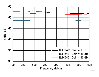
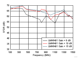
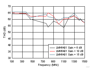
Figure 7-4, Figure 7-5, and Figure 7-6 show the analog signal chain performance of the cascaded LMH5401+LMH6401 path. Figure 7-7 shows the transformer coupling input performance with the ADC12DJ3200 ADC.
GUID-E575CA2D-E58B-416C-8FFA-4C2142A7D988-low.gif
LMH5401 Gain = 12 dB
Figure 7-4 SNR versus FREQ (LMH6401 I/P Path)
GUID-388A074C-D338-43E0-83BC-CE4A1C76AEEF-low.gif
LMH5401 Gain = 12 dB
Figure 7-5 SFDR versus FREQ (LMH6401 I/P Path)
GUID-723DD160-B6FF-4C27-9CB0-1C18B14689D8-low.gif
LMH5401 Gain = 12 dB
Figure 7-6 THD versus FREQ (LMH6401 I/P Path)
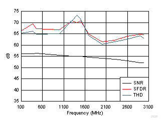
GUID-601611C4-B4E1-4D26-A3FD-989172E04562-low.gifFigure 7-7 SNR, SFDR, THD versus FREQ (TRANSFORMER I/P)

Figure 7-8 and Figure 7-9 show the measured spectrum of the TIDA-01022 design at a 997-MHz input signal for the LMH5401+LMH6401 combination and transformer coupling, respectively.
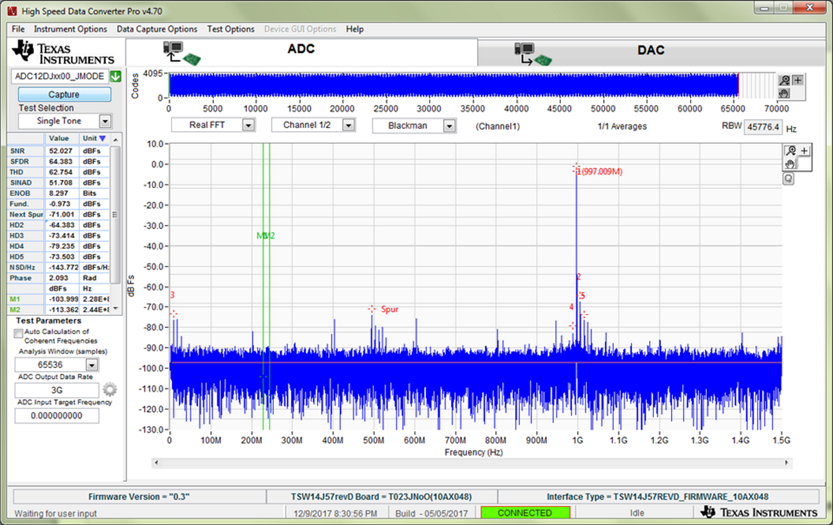
GUID-C5BC3A0D-BD65-4887-AFF8-3FA763BAB989-low.pngFigure 7-8 997-MHz Spectrum (LMH5401+LMH6401)
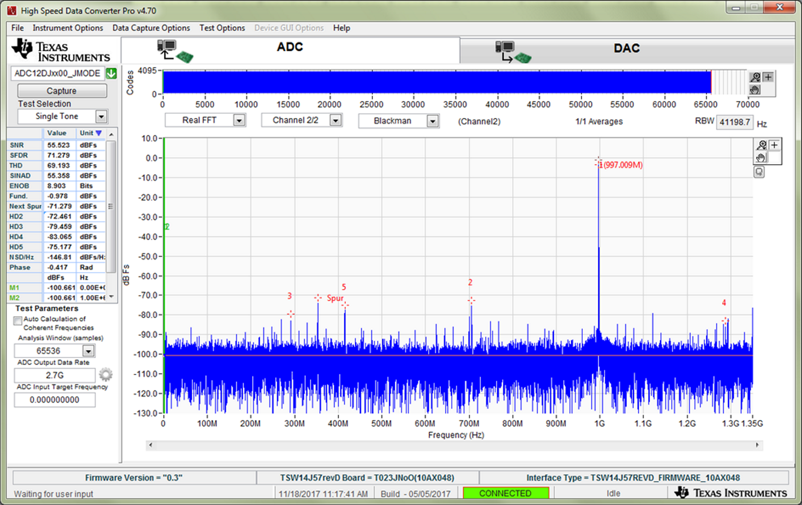
GUID-1C6789B6-C5E3-4591-9819-E52DD6625F59-low.pngFigure 7-9 997-MHz Spectrum (Transformer Coupling)