JAJU446A December   2017  – January 2022


  1.   概要
  2.   Resources
  3.   特長
  4.   アプリケーション
  5.   5
  6. System Description
    1. 1.1 Key System Specifications
  7. System Overview
    1. 2.1 Block Diagram
    2. 2.2 System-Level Description
    3. 2.3 Highlighted Products
      1. 2.3.1 Analog Signal Chain
        1. 2.3.1.1 LMH5401
        2. 2.3.1.2 LHM6401
        3. 2.3.1.3 BUF802
      2. 2.3.2 Clock
        1. 2.3.2.1 LMK61E2
        2. 2.3.2.2 LMK04828
        3. 2.3.2.3 LMX2594
      3. 2.3.3 Power
        1. 2.3.3.1 TPS82130
        2. 2.3.3.2 TPS7A84
    4. 2.4 System Design Theory
      1. 2.4.1 High-Speed, Low-Phase Noise Clock Generation
      2. 2.4.2 Channel-to-Channel Skew
      3. 2.4.3 Deterministic Latency
        1. 2.4.3.1 Importance of Deterministic Latency
      4. 2.4.4 Analog Front End
      5. 2.4.5 Multichannel System Power Requirement
      6. 2.4.6 Hardware Programming
  8. Circuit Design
    1. 3.1 Analog Input Front End
      1. 3.1.1 High-Input Impedance Buffer Implementation Using the BUF802
    2. 3.2 High-Speed Multichannel Clocking
    3. 3.3 Power Supply Section
      1. 3.3.1 DC-DC
        1. 3.3.1.1 How to Set 2.1-V Output Voltage
      2. 3.3.2 LDOs
  9. Host Interface
  10. Hardware Functional Block
  11. Getting Started Application GUI
  12. Testing and Results
    1. 7.1 Test Setup and Test Plan
    2.     44
    3. 7.2 SNR Measurement Test
    4. 7.3 Channel-to-Channel Skew Measurement Test
    5. 7.4 Performance Test Result
    6. 7.5 Multichannel Skew Measurement
    7. 7.6 49
  13. Design Files
    1. 8.1 Schematics
    2. 8.2 Bill of Materials
    3. 8.3 Altium Project
    4. 8.4 Gerber Files
    5. 8.5 Assembly Drawings
  14. Software Files
  15. 10Related Documentation
    1. 10.1 Trademarks
  16. 11About the Authors
    1. 11.1 Acknowledgment
  17. 12Revision History

Power Supply Section

Figure 3-10 shows the power supply tree of the reference design. The design requires an external +12-V DC power to generate 1.9 V and 1.1 V for the ADC; 3.3 V for the clocking devices (LMK61E2, LMK4828, and LMX2594); and ±2.5 V for the LMH5401 and LMH6401 amplifiers. This design has input overvoltage, overcurrent, high inrush current protection through eFuse (TPS259261), and an external bidirectional transient-voltage-suppression (TVS) diode (SMBJ15CA).
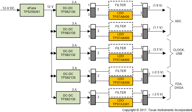
GUID-156EBB9E-775E-4FD6-8E3F-C34C70BB9CA0-low.gifFigure 3-10 TIDA-01022 Power Supply Block

The DC-DC converter and LDO generate the power supply rail, as Table 3-1 details.

Table 3-1 Power Supply Rail
Sl NUMBERTYPEPART NUMBERSUPPLY RAIL
1DC-DCTPS82130Intermediate rails for 3.3 V, 1.9 V, and 1.1 V
2LDOTPS7A84003.3 V, 1.9 V, and 1.1 V
3LDOTPS7A8300+2.5 V
4LDOTPS7A3301–2.5 V

The following subsections detail the design procedure for the various power supply rails.