JAJU446A December 2017 – January 2022
- 概要
- Resources
- 特長
- アプリケーション
- 5
- 1 System Description
- 2 System Overview
- 3 Circuit Design
- 4 Host Interface
- 5 Hardware Functional Block
- 6 Getting Started Application GUI
- 7 Testing and Results
- 8 Design Files
- 9 Software Files
- 10Related Documentation
- 11About the Authors
- 12Revision History
3.3.2 LDOs
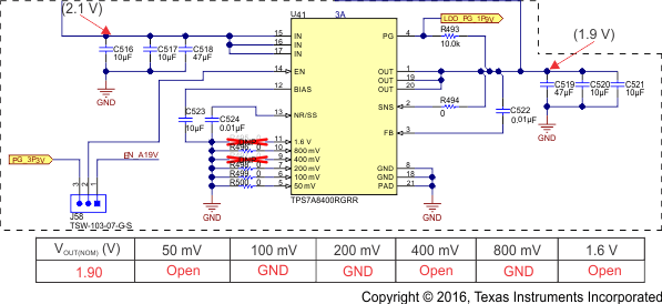
The TPS7A8400 is a positive-voltage (5-V), ultra-low-noise (4.4-μVRMS) LDO capable of sourcing a 3-A load with a low drop of 180 mV (see Figure 3-12). The TPS7A8x00 is designed primarily for high-accuracy, high-precision instrumentation applications where clean voltage rails are critical to maximize system performance. This feature makes the device ideal for powering operational amplifiers (op amps), ADCs, DACs, and other high-performance analog circuitry.
The TPS7A8400 has ANY-OUT™ programmable pins to program the desired output voltage. The sum of the internal reference voltage (VREF = 0.8 V) plus the accumulated sum of the respective voltage is assigned to each active pin. The ANY-OUT pins (pins 10, 7, and 6) are programmed to active low to obtain 1.9 V at the output. Other positive rails (1.1 V, 3.3 V, and 2.5 V) are similarly generated.
 Figure 3-12 LDO Power Supply Circuit (1.9-V Rail)
The TPS7A33 series of linear regulators are negative voltage (–36 V), ultra-low-noise (16-µVRMS, 72-dB power supply rejection ratio (PSRR)) linear regulators capable of sourcing a maximum load of 1 A. The output set resistors generate the –2.5 V.