JAJU446A December 2017 – January 2022
- 概要
- Resources
- 特長
- アプリケーション
- 5
- 1 System Description
- 2 System Overview
- 3 Circuit Design
- 4 Host Interface
- 5 Hardware Functional Block
- 6 Getting Started Application GUI
- 7 Testing and Results
- 8 Design Files
- 9 Software Files
- 10Related Documentation
- 11About the Authors
- 12Revision History
2.2 System-Level Description
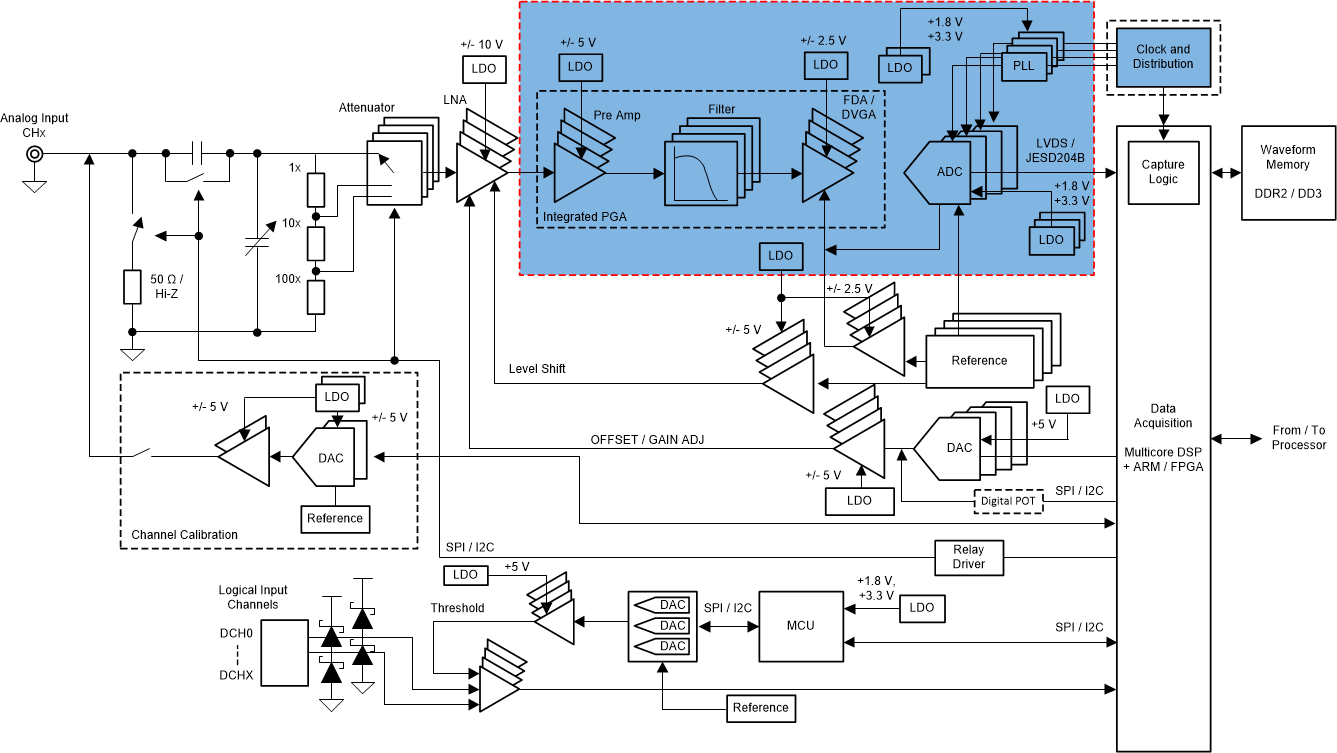
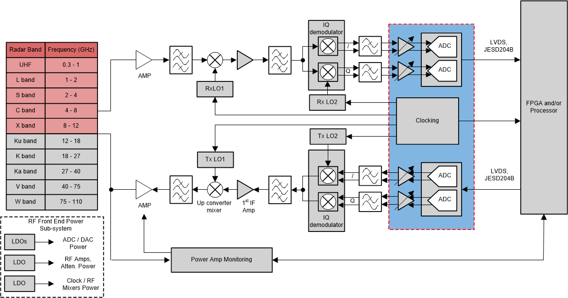
Figure 2-2, Figure 2-3, and Figure 2-4 show the subsystem block diagrams of the high-performance DSO, phase-array RADAR, and wireless tester, respectively. The AFE and system clocking architecture are highlighted in each diagram and are common across all three pieces of end equipment.
 Figure 2-2 High-Performance DSO AFE Subsystem
 Figure 2-3 RADAR RF Front-End Subsystem
 Figure 2-4 Wireless Tester AFE Subsystem
High-performance, multichannel digital storage oscilloscopes require a signal chain with a wideband AFE, high dynamic range, high SNR, and low channel-to-channel skew. The analog bandwidth is in the order of a 200-MHz to 5-GHz range and the sampling rate requires 5 Gsps to 10 Gsps.
Wireless testers require high dynamic range and wideband receivers to test 5G and later standards for wireless compliant equipment. These testers require a new high-performance DAC and ADC to obtain the true performance for high accuracy. The requirement of higher data capacity and user data demands a higher carrier frequency compared to the cellular implementation below 6 GHz of today. At the time of this writing, the final specifications for the 5G standard is not available; however, a bandwidth around 500 MHz to 2 GHz is currently under consideration.
Phased-array radar applications require a high dynamic range, wide receiver bandwidth, low latency, and good synchronization between the channels. This reference design front end covers the RADAR lower-band range from 0.3 GHz to 4 GHz (UHF, L band, and S band).