SBOS527G December 2010 – September 2025 TMP411-Q1 , TMP411D-Q1
PRODUCTION DATA
- 1
- 1 Features
- 2 Applications
- 3 Description
- 4 Device Comparison
- 5 Pin Configuration and Functions
-
6 Specifications
- 6.1 Absolute Maximum Ratings
- 6.2 ESD Ratings
- 6.3 Recommended Operating Conditions
- 6.4 Thermal Information
- 6.5 Electrical Characteristics (TMP411-Q1)
- 6.6 Electrical Characteristics (TMP411D-Q1)
- 6.7 Timing Characteristics
- 6.8 Timing Diagrams
- 6.9 Typical Characteristics (TMP411-Q1)
- 6.10 Typical Characteristics (TMP411D-Q1)
- 7 Detailed Description
-
8 Register Map
- 8.1 Register Information
- 8.2 Pointer Register
- 8.3 Temperature Registers
- 8.4 Limit Registers
- 8.5 Status Register
- 8.6 Configuration Register
- 8.7 Resolution Register
- 8.8 Conversion Rate Register
- 8.9 N-factor Correction Register
- 8.10 Minimum and Maximum Registers
- 8.11 Consecutive Alert Register
- 8.12 THERM Hysteresis Register
- 8.13 Identification Registers
- 9 Application and Implementation
- 10Device and Documentation Support
- 11Revision History
- 12Mechanical, Packaging, and Orderable Information
Package Options
Mechanical Data (Package|Pins)
- DDF|8
Thermal pad, mechanical data (Package|Pins)
Orderable Information
9.2.1 Design Requirements
The TMP411-Q1 and TMP411D-Q1 devices are designed to be used with discrete transistors or substrate transistors built into processor chips and ASICs. NPN or PNP transistors can be used, as long as the base-emitter junction is the remote temperature sensor. A transistor or diode connection can be used, as shown in Figure 7-1. The D+ pin waveform is shown in Figure 9-3 while a transistor is connected between the D+ and D– pins. Due to the three different source currents used in Section 7.2, the D+ waveform has three levels of voltage during temperature conversion.
 Figure 9-3 D+ Waveform
Errors in remote temperature sensor readings are the result of the ideality factor and current excitation from the TMP411-Q1 and TMP411D-Q1 versus the manufacturer-specified operating current for a given transistor. Some manufacturers specify a high-level and low-level current for the temperature-sensing substrate transistors. The TMP411-Q1 and TMP411D-Q1 have an ILOW value of 6μA, and an IHIGH value of 120μA. The TMP411-Q1 and TMP411D-Q1 allow for different n-factor values, as shown in Table 8-6.
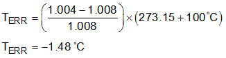
The ideality factor (n) is a measured characteristic of a remote temperature sensor diode compared to an ideal diode. The ideality factor reduces to a value of 1.008. For transistors with an ideality factor that does not match the TMP411-Q1 and TMP411D-Q1, Equation 4 calculates the temperature error. Note that the actual temperature (°C) must be converted to Kelvin (K) for the equation to yield the correct results.
 or
or
where:
- n or nactual = the ideality factor of the remote temperature sensor
- T(°C) or Tactual(°C) = actual temperature
- TERR = Treported - Tactual= device reading error due to n or nactual ≠ 1.008
- Degree delta is the same for °C and K
- nexpected = 1.008
For n = 1.004 and T(°C) = 100°C, use Equation 5:
If a discrete transistor is used as the remote temperature sensor, please select the transistor according to the following criteria, which results in the best accuracy.
- Base-emitter voltage > 0.25V at 6µA, at the highest sensed temperature.
- Base-emitter voltage < 0.95V at 120µA, at the lowest sensed temperature.
- Base resistance < 100Ω
- Tight control of VBE characteristics is indicated by small variations in hFE (that is, 50 to 150).
Based on these criteria, use two small-signal transistors, such as the 2N3904 (NPN) or 2N3906 (PNP).