SLAA559E April 2014 – November 2016 MSP430AFE221 , MSP430AFE222 , MSP430AFE223 , MSP430AFE231 , MSP430AFE232 , MSP430AFE233 , MSP430AFE251 , MSP430AFE252 , MSP430AFE253 , MSP430F2001 , MSP430F2002 , MSP430F2003 , MSP430F2011 , MSP430F2012 , MSP430F2013 , MSP430F2013-EP , MSP430F2101 , MSP430F2111 , MSP430F2112 , MSP430F2121 , MSP430F2122 , MSP430F2131 , MSP430F2132 , MSP430F2232 , MSP430F2234 , MSP430F2252 , MSP430F2254 , MSP430F2272 , MSP430F2274 , MSP430F233 , MSP430F2330 , MSP430F235 , MSP430F2350 , MSP430F2370 , MSP430F2410 , MSP430F2416 , MSP430F2417 , MSP430F2418 , MSP430F2419 , MSP430F247 , MSP430F2471 , MSP430F248 , MSP430F2481 , MSP430F249 , MSP430F2491 , MSP430F2616 , MSP430F2617 , MSP430F2618 , MSP430F2619 , MSP430FR5847 , MSP430FR58471 , MSP430FR5848 , MSP430FR5849 , MSP430FR5857 , MSP430FR5858 , MSP430FR5859 , MSP430FR5867 , MSP430FR58671 , MSP430FR5868 , MSP430FR5869 , MSP430FR5870 , MSP430FR5872 , MSP430FR58721 , MSP430FR5887 , MSP430FR5888 , MSP430FR5889 , MSP430FR58891 , MSP430FR5922 , MSP430FR59221 , MSP430FR5947 , MSP430FR59471 , MSP430FR5948 , MSP430FR5949 , MSP430FR5957 , MSP430FR5958 , MSP430FR5959 , MSP430FR5967 , MSP430FR5968 , MSP430FR5969 , MSP430FR59691 , MSP430FR5970 , MSP430FR5972 , MSP430FR59721 , MSP430FR5986 , MSP430FR5987 , MSP430FR5988 , MSP430FR5989 , MSP430FR5989-EP , MSP430FR59891 , MSP430FR5994 , MSP430FR6820 , MSP430FR6822 , MSP430FR68221 , MSP430FR6870 , MSP430FR6872 , MSP430FR68721 , MSP430FR6877 , MSP430FR6879 , MSP430FR68791 , MSP430FR6887 , MSP430FR6888 , MSP430FR6889 , MSP430FR68891 , MSP430FR6920 , MSP430FR6922 , MSP430FR69221 , MSP430FR6927 , MSP430FR69271 , MSP430FR6928 , MSP430FR6970 , MSP430FR6972 , MSP430FR69721 , MSP430FR6977 , MSP430FR6979 , MSP430FR69791 , MSP430FR6987 , MSP430FR6988 , MSP430FR6989 , MSP430FR69891 , MSP430G2001 , MSP430G2101 , MSP430G2102 , MSP430G2111 , MSP430G2112 , MSP430G2121 , MSP430G2131 , MSP430G2132 , MSP430G2152 , MSP430G2153 , MSP430G2201 , MSP430G2202 , MSP430G2203 , MSP430G2210 , MSP430G2211 , MSP430G2212 , MSP430G2213 , MSP430G2221 , MSP430G2230 , MSP430G2231 , MSP430G2232 , MSP430G2233 , MSP430G2252 , MSP430G2253 , MSP430G2302 , MSP430G2303 , MSP430G2312 , MSP430G2313 , MSP430G2332 , MSP430G2333 , MSP430G2352 , MSP430G2353 , MSP430G2402 , MSP430G2403 , MSP430G2412 , MSP430G2413 , MSP430G2432 , MSP430G2433 , MSP430G2452 , MSP430G2453 , MSP430G2513 , MSP430G2533 , MSP430G2553
-
Migrating from the MSP430F2xx and MSP430G2xx Families to the MSP430FR58xx/FR59xx/68xx/69xx Family
- Trademarks
- 1 Introduction
- 2 In-System Programming of Nonvolatile Memory
- 3 Hardware Migration Considerations
- 4 Device Calibration Information
- 5 Important Device Specifications
- 6 Core Architecture Considerations
- 7 Peripheral Considerations
- 8 Conclusion
- 9 References
- Revision History
6.1 Power Management Module (PMM)
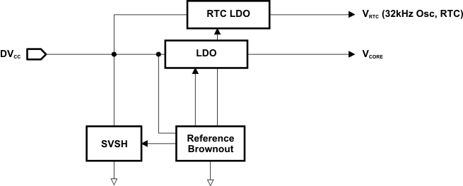
The F2xx family of devices use a single voltage rail to power the chip; that is, a single power rail supplies both the analog peripherals and the digital core on the chip. The FR59xx family uses a split voltage supply. The external voltage supply on the DVCC pin is fed to an internal low-dropout voltage regulator (LDO) that supplies the CPU, memories, and digital modules, while AVCC supplies the analog modules (see Figure 1).
The PMM manages all functions related to the core voltage and its supervision. Its primary functions are, first, to generate a supply voltage for the core logic and, second, to provide several mechanisms for the supervision of both the voltage supplied to the device (DVCC) and the voltage generated for the core (VCORE).
 Figure 1. PMM Block Diagram
 Using a split supply is especially advantageous as it allows the core to operate at a lower voltage, which brings significant power savings. It also ensures that the core receives a stable and regulated voltage over a wide supply range.
This allows the FR59xx devices to operate across the entire voltage range of the device at the maximum device frequency of 16 MHz. In comparison, F2xx devices have a relationship between system frequency and supply voltage that must be adhered to in order to ensure proper operation of the device.
Because supply voltage supervision is an important aspect of providing a stable supply or a notification in case of power failure, the FR59xx provides an high-side supply voltage supervision (SVSH) block. The SVSH handles the supervision of the external chip supply (DVCC), the low-side supervision of the core is handled internally by the PMM.
The SVS threshold tracks directly with the device minimum supply of 1.8 V, and there is no need to program SVS high-side levels as in the F2xx family (in which the SVS feature is available on select devices only). Also, the SVSH block in the FR59xx is highly simplified. It is on by default at power-up and stays on in active, LPM0, LPM1, and LPM2 modes. It can be turned off in LPM3, LPM4, and LPMx.5 modes, if required.
A useful feature in the FR59xx family is the ability to trigger an NMI when the supply falls below the SVS level. This is useful, for example, if a battery-powered application is low on charge. In this case, an interrupt can be used to configure ports to consume the least power and set the device in LPM3.5, consuming approximately 500 nA to maximize battery life while preserving RTC for as long as possible. The interrupt can also be used to warn the end user about the low battery state and to power down gracefully.
One of the main differences between the two families that can be observed while debugging can be attributed to the PMM module. In the FR59xx family, the VCOREregulator operates in two modes to conserve power: high-performance mode (used in active, LPM0, and LPM1 modes) and low-power mode (used in LPM2, LPM3, and LPM4 modes). When the FR59xx device is plugged into the debugger, it automatically forces the LDO to the high-performance mode regardless of the operating mode (active or LPM) that is set by the application code. In an application, this affects current consumption and wake-up times, which may cause the device to behave differently between stand-alone and debugger modes. When debugging with any of the lower LPMs (LPM2, LPM3, and LPM4), ensure that the debugger is disconnected to observe device performance accurately.