SLASFL3 September   2026 DAC90802

PRODUCTION DATA  

  1.   1
  2. 1 Features
  3. 2 Applications
  4. 3 Description
  5. 4 Pin Configuration and Functions
  6. 5 Specifications
    1. 5.1 Absolute Maximum Ratings
    2. 5.2 ESD Ratings
    3. 5.3 Recommended Operating Conditions
    4. 5.4 Thermal Information
    5. 5.5 Electrical Characteristics
    6. 5.6 Timing Requirements
    7. 5.7 Timing Diagrams
    8. 5.8 Typical Characteristics
      1. 5.8.1 Typical Characteristics: Linearity
      2. 5.8.2 Typical Characteristics: Glitch
      3. 5.8.3 Typical Characteristics: Multiplying Mode
      4. 5.8.4 Typical Characteristics: Fast-Settling Mode
      5. 5.8.5 Typical Characteristics: AWG Mode
  7. 6 Detailed Description
    1. 6.1 Overview
    2. 6.2 Functional Block Diagram
    3. 6.3 Feature Description
      1. 6.3.1 Digital-to-Analog Converters
        1. 6.3.1.1 Reference
        2. 6.3.1.2 Output Span
          1. 6.3.1.2.1 Gain Overrange
        3. 6.3.1.3 Output Synchronization
        4. 6.3.1.4 Thermal Sensors
      2. 6.3.2 Power-On
      3. 6.3.3 Serial Data Interface
        1. 6.3.3.1 SPI Configurations
        2. 6.3.3.2 SPI Stream Mode
        3. 6.3.3.3 SPI Daisy Chain Mode
    4. 6.4 Device Functional Modes
      1. 6.4.1 AWG Mode
      2. 6.4.2 Fast Settling Mode
      3. 6.4.3 Multiplying Mode
  8. 7 Register Maps
    1. 7.1 COMMON Registers
    2. 7.2 HS_DATA Registers
    3. 7.3 HR_DATA Registers
  9. 8 Application and Implementation
    1. 8.1 Application
    2. 8.2 Design Requirements
      1. 8.2.1 Reference Signal Chain Information
        1. 8.2.1.1 DC Reference
        2. 8.2.1.2 AC Reference
      2. 8.2.2 Optimising the Self-Heating Trim to Achieve Lowest THD Across Frequencies for High Voltage Swing
      3. 8.2.3 Digital Interface
      4. 8.2.4 Grounding Recommendations
    3. 8.3 Power Supply Recommendations
    4. 8.4 Layout
      1. 8.4.1 Layout Recommendation
      2. 8.4.2 Layout Example
  10. 9 Device and Documentation Support
    1. 9.1 Related Documentation
    2. 9.2 Receiving Notification of Documentation Updates
    3. 9.3 Support Resources
    4. 9.4 Trademarks
    5. 9.5 Electrostatic Discharge Caution
    6. 9.6 Glossary
  11. 10Revision History
  12. 11Mechanical, Packaging, and Orderable Information

Typical Characteristics: Fast-Settling Mode

at TA = –40°C to +125°C, VCC = +8.5V to +23.5V, VEE = –8.5V to –23.5V, AVDD = 5.0V, DVDD = 1.5V, LVDD = 1.5V, VIO = 1.5V, VOSADJ_ENx = 0, OFS_ENx = 0, ROFS_F = ROFS_S = VOSADJ = AGND see note for VREFP and VREFN, and all typical values at TA = 25°C, output unloaded (unless otherwise noted)

DAC90802 Digital Feedthrough Zoomed In
Bipolar mode, REFP = +5V, REFN = –5V
Figure 5-43 Digital Feedthrough Zoomed In
DAC90802 Settling Time to 0.1% FSR
Gain = 1, reference: ±5V, rising step of: 100mV
Figure 5-45 Settling Time to 0.1% FSR
DAC90802 Settling Time to 0.0015% FSR
Gain = 1, reference: ±5V, rising step of: 100mV
Figure 5-47 Settling Time to 0.0015% FSR
DAC90802 Settling Time to 0.0004% FSR
Gain = 1, reference: ±5V, rising step of: 100mV
Figure 5-49 Settling Time to 0.0004% FSR
DAC90802 Settling Time to 0.1% FSR
Gain = 1, reference: ±5V, rising step of: 10V
Figure 5-51 Settling Time to 0.1% FSR
DAC90802 Settling Time to 0.0015% FSR
Gain = 1, reference: ±5V, rising step of: 10V
Figure 5-53 Settling Time to 0.0015% FSR
DAC90802 Settling Time to 0.0004% FSR
Gain = 1, reference: ±5V, rising step of: 10V
Figure 5-55 Settling Time to 0.0004% FSR
DAC90802 Settling Time to 0.1% FSR
Gain = 1, reference: ±20V, rising step of: 40V
Figure 5-57 Settling Time to 0.1% FSR
DAC90802 Settling Time to 0.0015% FSR
Gain = 1, reference: ±20V, rising step of: 40V
Figure 5-59 Settling Time to 0.0015% FSR
DAC90802 Settling Time to 0.0004% FSR
Gain = 1, reference: ±20V, rising step of: 40V
Figure 5-61 Settling Time to 0.0004% FSR
DAC90802 Output Noise vs Frequency
Gain = 1, excluding R1x and R2x resistors, bipolar
Figure 5-63 Output Noise vs Frequency
DAC90802 0.1Hz to 10Hz Flicker Noise
Gain = 1, bipolar mode
Figure 5-65 0.1Hz to 10Hz Flicker Noise
DAC90802 VCC
                                                  PSRR vs Frequency
REFPx = +5V, REFNx = –5V, bipolar mode
Figure 5-67 VCC PSRR vs Frequency
DAC90802 AVDD PSRR vs Frequency
REFPx = +5V, REFNx = –5V, bipolar mode
Figure 5-69 AVDD PSRR vs Frequency
DAC90802 Slew Rate vs Output Voltage Step, Bipolar
REFPx = +5V, REFNx = –5V
Figure 5-71 Slew Rate vs Output Voltage Step, Bipolar
DAC90802 Digital Feedthrough Zoomed Out
Bipolar mode, REFP = +5V, REFN = –5V
SCLK = 1MHz, midcode
Figure 5-44 Digital Feedthrough Zoomed Out
DAC90802 Settling Time to 0.1% FSR
Gain = 1, reference: ±5V, falling step of: 100mV
Figure 5-46 Settling Time to 0.1% FSR
DAC90802 Settling Time to 0.0015% FSR
Gain = 1, reference: ±5V, falling step of: 100mV
Figure 5-48 Settling Time to 0.0015% FSR
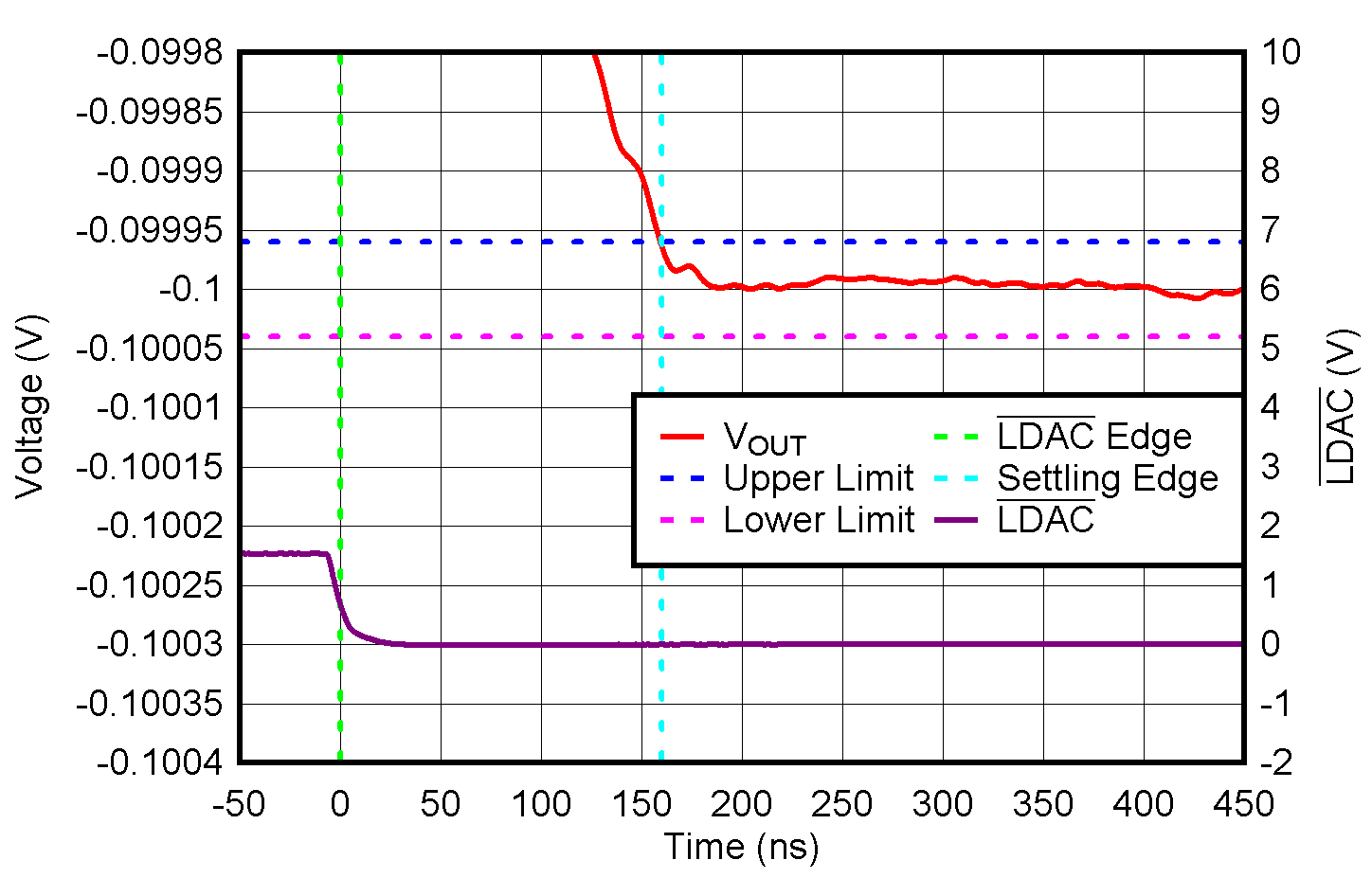
DAC90802 Settling Time to 0.0004% FSR
Gain = 1, reference: ±5V, falling step of: 100mV
Figure 5-50 Settling Time to 0.0004% FSR
DAC90802 Settling Time to 0.1% FSR
Gain = 1, reference: ±5V, falling step of: 10V
Figure 5-52 Settling Time to 0.1% FSR
DAC90802 Settling Time to 0.0015% FSR
Gain = 1, reference: ±5V, falling step of: 10V
Figure 5-54 Settling Time to 0.0015% FSR
DAC90802 Settling Time to 0.0004% FSR
Gain = 1, reference: ±5V, falling step of: 10V
Figure 5-56 Settling Time to 0.0004% FSR
DAC90802 Settling Time to 0.1% FSR
Gain = 1, reference: ±20V, falling step of: 40V
Figure 5-58 Settling Time to 0.1% FSR
DAC90802 Settling Time to 0.0015% FSR
Gain = 1, reference: ±20V, falling step of: 40V
Figure 5-60 Settling Time to 0.0015% FSR
DAC90802 Settling Time to 0.0004% FSR
Gain = 1, reference: ±20V, falling step of: 40V
Figure 5-62 Settling Time to 0.0004% FSR
DAC90802 Output Noise vs Frequency
Gain = 4, excluding R1x and R2x resistors, bipolar
Figure 5-64 Output Noise vs Frequency
DAC90802 0.1Hz to 10Hz Flicker Noise
Gain = 4, bipolar mode
Figure 5-66 0.1Hz to 10Hz Flicker Noise
DAC90802 VEE
                                                  PSRR vs Frequency
REFPx = +5V, REFNx = –5V, bipolar mode
Figure 5-68 VEE PSRR vs Frequency
DAC90802 LVDD PSRR vs Frequency
REFPx = +5V, REFNx = –5V, bipolar mode
Figure 5-70 LVDD PSRR vs Frequency