SLVAE57B February 2021 – October 2021 LM5050-1 , LM5050-2 , LM5051 , LM66100 , LM74202-Q1 , LM74500-Q1 , LM74610-Q1 , LM74700-Q1 , LM74720-Q1 , LM74721-Q1 , LM74722-Q1 , LM7480-Q1 , LM7481-Q1 , LM76202-Q1 , SM74611 , TPS2410 , TPS2411 , TPS2412 , TPS2413 , TPS2419
- Trademarks
- 1 Introduction
- 2 Reverse Battery Protection
- 3 ORing Power Supplies
- 4 Reverse Battery Protection using MOSFETs
- 5 Reverse Polarity Protection vs Reverse Current Blocking
- 6 What is an Ideal Diode Controller?
- 7 Automotive Transient protection with Ideal Diode Controllers
- 8 ORing Power Supplies with Ideal Diode Controllers
- 9 Integrated Ideal Diode Solution
- 10Summary
- 11References
- 12Revision History
6.6.3 TVSless Operation
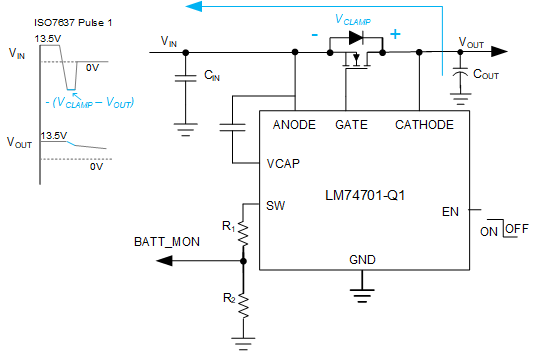
The increase in processing power levels and miniaturized electronic system sizes has increased the demand for high efficiency and high power density designs. This poses new challenges for system designers particularly in designing automotive front-end protection systems. Devices such as LM74701-Q1 and LM74721-Q1 enable a smaller solution size and lower cost, making these devices suitable for designing input reverse polarity protection of space constrained applications such as ADAS camera modules. These devices use integrated active clamping to limit the input voltage levels during negative transient pulses. When the voltage across Drain and Source of the external MOSFET reaches VDSCLAMP level, the external MOSFET is operated in saturation region, operating as an active clamp element and dissipates transient pulse energy of events such as ISO7637-2 pulse 1 negative transient. During the VDS clamp operation device allows flow of reverse current from output capacitor back to the input source. VDS clamp threshold is selected such that it does not engage into VDS clamp mode for automotive EMC tests where reverse current blocking is needed such as AC superimpose performance (LV124,E-06, ISO16750-2) and Input micro short interruption events (LV124, E-10) ensuring robust EMC performance. For further details on how to design input-side TVS-less reverse polarity protection solution, refer to data sheet LM74701-Q1
 Figure 6-8 LM74701-Q1 Operation During VDS Clamp Mode
In applications such as body control module load driving paths, where input reverse polarity protection is required but reverse current blocking is not a must-have requirement, LM74501-Q1 enables TVSless operation using a gate discharge timer feature, offering space and price advantages. For further details, refer to LM74501 data sheet.