SLVAE57B February 2021 – October 2021 LM5050-1 , LM5050-2 , LM5051 , LM66100 , LM74202-Q1 , LM74500-Q1 , LM74610-Q1 , LM74700-Q1 , LM74720-Q1 , LM74721-Q1 , LM74722-Q1 , LM7480-Q1 , LM7481-Q1 , LM76202-Q1 , SM74611 , TPS2410 , TPS2411 , TPS2412 , TPS2413 , TPS2419
- Trademarks
- 1 Introduction
- 2 Reverse Battery Protection
- 3 ORing Power Supplies
- 4 Reverse Battery Protection using MOSFETs
- 5 Reverse Polarity Protection vs Reverse Current Blocking
- 6 What is an Ideal Diode Controller?
- 7 Automotive Transient protection with Ideal Diode Controllers
- 8 ORing Power Supplies with Ideal Diode Controllers
- 9 Integrated Ideal Diode Solution
- 10Summary
- 11References
- 12Revision History
9 Integrated Ideal Diode Solution
For lower voltage applications, such as backup battery solutions, an integrated ideal diode solution can be used. The LM66100 uses a P-channel MOSFET and integrates the functionality of an ideal diode into a single device.
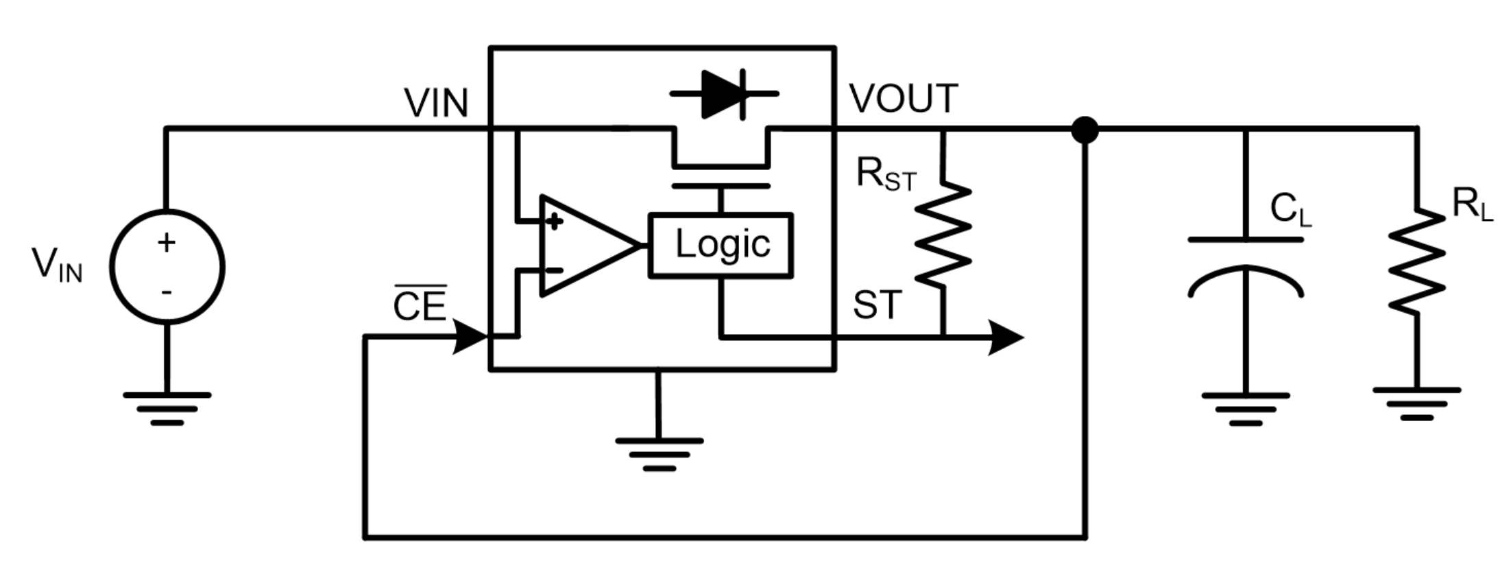
A typical application schematic in Figure 9-1 shows the LM66100 ideal diode in a reverse current blocking (RCB) circuit. The chip enable works by comparing the CE pin voltage to the input voltage. When the CE pin voltage is higher than VIN, the device is disabled and the PMOS is turned off. When the CE pin voltage is lower than VIN, then the MOSFET is on and the device operates with low forward voltage drop. By connecting the CE pin to VOUT in this configuration, this ensures that the MOSFET is disabled whenever the output voltage is forced higher than the input voltage. The LM66100 integrated ideal diode also integrates reverse polarity/battery protection, which helps to prevent damage to the upstream battery if it is wired incorrectly.
 Figure 9-1 LM66100 Reverse Current Blocking Circuit
 Figure 9-2 Reverse Current Blocking Waveform
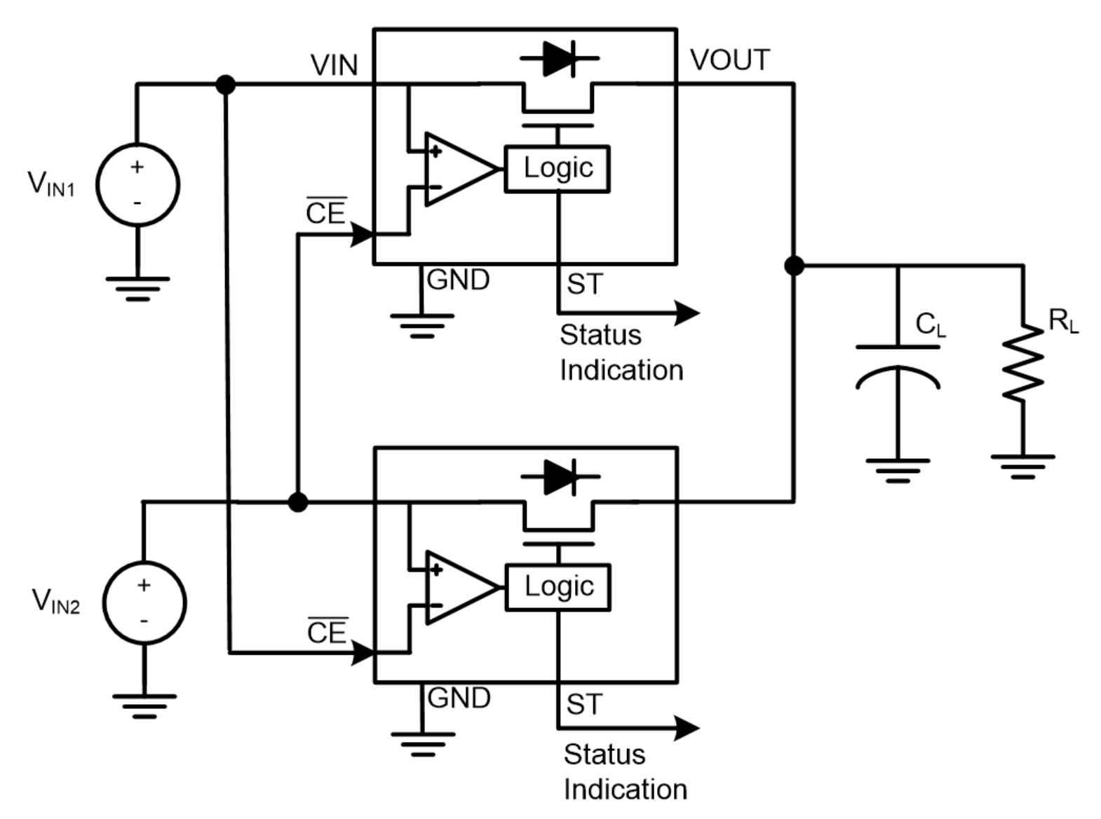
Similar to the ideal diode controllers, the LM66100 can also be used in redundant power architectures for ORing between power supplies. By using two LM66100s with the CE pins tied to the other input voltage channel. This ensures that the highest input supply voltage is selected as the output. Since the highest supply is always be selected, the solution allows for a make-before-break configuration, which prevents any reverse current flow between the input supplies.
 Figure 9-3 LM66100 ORing Solution
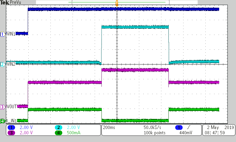
Figure 9-4 shows a typical switchover event from VIN1 to VIN2. During this switchover event, VIN1 decays causing the LM66100 to switch to VIN2, while blocking reverse current from entering VIN1.
 Figure 9-4 LM66100 Switchover from IN1 to IN2
The LM66100 integrated ideal diode also contains the same advantages as the ideal diode controllers, when compared to a discrete diode or FET solution. During normal operation, the LM66100 has a lower forward conduction loss when compared to a discrete diode. Instead of operating with the normal 0.3 V–0.4 V drop of a discrete diode, the power loss across the LM66100 is minimized across the MOSFET instead. This results in a lower power dissipation, leading to a higher power savings for applications.
The LM66100 also has a fast reverse voltage recovery time when compared to a discrete FET. While a discrete FET does not turn off until the voltage drops below the VTH of the FET, the LM66100 stops reverse current within tOFF once the voltage on the output rises above the input. This helps prevent output capacitors from discharging current back into the upstream supply, which can damage components such as input batteries or PSUs.
| FEATURE | IDEAL DIODE CONTROLLER | LM66100 | DISCRETE DIODE | DISCRETE FET |
|---|---|---|---|---|
| Low Power Dissipation | ✓ | ✓ | ✓ | |
| Low Reverse Leakage Current | ✓ | ✓ | ✓ | |
| Reverse Polarity Protection | ✓ | ✓ | ✓ | *(additional components)* |