SLVAE85A February 2019 – September 2025 LM1117-Q1 , LM317 , LP2951 , LP2951-Q1 , LP2985 , TL1963A , TL1963A-Q1 , TLV1117 , TLV709 , TLV755P , TLV761 , TLV766-Q1 , TLV767 , TLV767-Q1 , TPS709 , TPS709-Q1 , TPS715 , TPS745 , TPS7A16A , TPS7A16A-Q1 , TPS7A25 , TPS7A26 , TPS7A43 , TPS7A44 , TPS7A47 , TPS7A47-Q1 , TPS7A49 , TPS7B63-Q1 , TPS7B68-Q1 , TPS7B69-Q1 , TPS7B81 , TPS7B81-Q1 , TPS7B82-Q1 , TPS7B83-Q1 , TPS7B84-Q1 , TPS7B85-Q1 , TPS7B86-Q1 , TPS7B87-Q1 , TPS7B88-Q1 , TPS7B91 , TPS7B92 , TPS7C84-Q1 , UA78L , UA78M , UA78M-Q1
- 1
- An empirical analysis of the impact of board layout on LDO thermal performance
- Trademarks
- 1Introduction
- 2Procedure
- 3Test Results and Discussion
- 4Conclusion
- 5Future Study
- 6References
- 7Revision History
- A Thermal Test Board Layouts
- B Thermal Test Results
1 Introduction
LDOs are the most common DC/DC converter in electronic power designs due to their relative simplicity and cost advantage. As applications become increasingly integrated and compact, power designs must become smaller and cheaper, resulting in more LDO content. As a result, thermal performance is an even more important system design factor as LDOs are linear converters and inherently power dissipative. While JEDEC has standardized the method to measure and report semiconductor thermal metrics in a uniform manner, the standard is not fully optimized for thermal performance. One of the most significant factors that affects thermal performance falls on the system designer, PCB layout. The goal of this application report is to aid these designers by investigating the effect of PCB layout on the thermal performance of LDOs. Although the LDOs thermal performance in small SMD packages application report and the AN-1520 a guide to board layout for best thermal resistance for exposed packages application report previously discussed this topic, this study aims to be more applicable by collecting data in a functional setting. This setting includes functional PCB layouts with passive components that emulate TI Evaluation Modules (EVMs), and thermal measurements taken through active powering. Active powering refers to placing the LDO in a normal operation and varying the input voltage and the load current to increase the power dissipation and generate heat at the junction of the device.
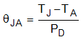
The most popular metric for evaluating semiconductor thermal performance is the junction-to-ambient thermal resistance, θJA. Equation 1 shows that this parameter is defined as the difference between the operating temperature and junction temperature of a device per watt of power dissipated in the device:
A design with a smaller θJA has a lower junction temperature for a given level of power dissipation, improving longevity and reliability. Semiconductor and IC package thermal metrics application report explains that the two factors that have a large impact on θJA are the PCB layout and IC package. Three LDOs in common packages, the TPS745 (WSON package), TPS7B82-Q1 (TO-252 package), and TLV755P (SOT-23 package) are tested with five different PCB layouts and are chosen to investigate how much these two factors affect thermal performance.
The dependence of semiconductor thermal performance on additional external factors including air flow, altitude, and ambient temperature has resulted in the need for JEDEC to standardize measurement procedures and test boards for θJA and other thermal metrics. For this application report, approximations of the Low Effective Thermal Conductivity Test Board, described in https://www.jedec.org/system/files/docs/JESD51-3.PDF, and the High Effective Thermal Conductivity Test Board, described in https://www.jedec.org/system/files/docs/jesd51-7.PDF, are designed for each package along with three custom layouts. The area and layer stack of each board follow the JEDEC standard test board approximations: 4layer PCBs with an area of 9-in2 (3-in by 3-in). The outer layers contain two ounce copper thickness while the inner layers contain one ounce copper thickness. The five layouts fabricated for each package contain increasing amounts of copper connected to the device with the intent to measure θJA and show an inverse relationship versus copper coverage. To improve the consistency of the results across the three packages, the amount of copper used for heat sinking in each type of layout is kept equal. In order of least to greatest copper content, the layout types are referred to as:
- 1S0P Approximation
- Internally Disconnected
- JEDEC High-K Approximation
- Thermally Enhanced
- Thermally Saturated
Thermal vias are also included in the thermal landing pad for all WSON and TO-252 layouts according to the JEDEC standard specified in https://www.jedec.org/system/files/docs/JESD51-9.pdf. These vias have a 20 millimeter (mm) diameter, 10-mm hole size, and 17-µm copper plating.
Two different θJA values are used as benchmarks for comparison. The first is θJA, datasheet as specified in the Thermal Information table in the datasheet of each device as RθJA. θJA, datasheet is derived using a thermal model of the JEDEC High-K Thermal Test Board and is the most popular metric used by designers to evaluate thermal performance. The second value is θJA,1S0P, as measured with the 1S0P Approximation layout. This value provides an example of the expected thermal performance for a worst-case layout. Figure 1-1 through Figure 1-5 show 3D generated images for each of the layouts designed for the TPS745 in the WSON package. Drawings of all four layers for each layout can be found in Appendix A. Table 1-1 provides descriptions for each design layout and copper coverage.
| BOARD | ATTRIBUTE | DESCRIPTION | CONNECTED COPPER AREA(in2) | DISCONNECTED COPPER AREA(in2) |
|---|---|---|---|---|
| 1S0P Approximation | Top Layer | Traces only | None | None |
| Internal Layer 1 | No copper | |||
| Internal Layer 2 | No copper | |||
| Bottom Layer | Traces only | |||
| Additional Thermal Vias | None | |||
| Internally Disconnected | Top Layer | Traces only | 0.07 | 16.8 |
| Internal Layer 1 | Medium, unconnected, discontinuous planes (1) | |||
| Internal Layer 2 | Medium, unconnected, discontinuous planes (1) | |||
| Bottom Layer | Traces and one small ground plane | |||
| Additional Thermal Vias | None | |||
| JEDEC High-K Approximation | Top Layer | Traces only | 10.2 | 8.53 |
| Internal Layer 1 | One large ground plane | |||
| Internal Layer 2 | Traces and one large, unconnected plane | |||
| Bottom Layer | One medium ground plane | |||
| Additional Thermal Vias | None | |||
| Thermally Enhanced | Top Layer | Traces and one small ground plane | 10.5 | 8.43 |
| Internal Layer 1 | Small ground plane and two unconnected planes | |||
| Internal Layer 2 | Traces and one medium ground plane | |||
| Bottom Layer | One medium ground plane | |||
| Additional Thermal Vias | Only around the device | |||
| Thermally Saturated | Top Layer | Large ground and power planes | 34.1 | None |
| Internal Layer 1 | One large ground plane | |||
| Internal Layer 2 | Traces and one large ground plane | |||
| Bottom Layer | One large ground plane | |||
| Additional Thermal Vias | Around the device and throughout the PCB |
 1S0P Approximation Layout") Figure 1-1 TPS745 (WSON) 1S0P Approximation Layout
Figure 1-1 TPS745 (WSON) 1S0P Approximation Layout Internally Disconnected Layout") Figure 1-2 TPS745 (WSON) Internally Disconnected Layout
Figure 1-2 TPS745 (WSON) Internally Disconnected Layout JEDEC High-K Approximation Layout") Figure 1-3 TPS745 (WSON) JEDEC High-K Approximation Layout
Figure 1-3 TPS745 (WSON) JEDEC High-K Approximation Layout Thermally Enhanced Layout") Figure 1-4 TPS745 (WSON) Thermally Enhanced Layout
Figure 1-4 TPS745 (WSON) Thermally Enhanced Layout Thermally Saturated Layout") Figure 1-5 TPS745 (WSON) Thermally Saturated Layout
Figure 1-5 TPS745 (WSON) Thermally Saturated Layout