SPRACX0 March 2021 F29H850TU , F29H859TU-Q1 , TMS320F280021 , TMS320F280021-Q1 , TMS320F280023 , TMS320F280023-Q1 , TMS320F280023C , TMS320F280025 , TMS320F280025-Q1 , TMS320F280025C , TMS320F280025C-Q1 , TMS320F280040-Q1 , TMS320F280040C-Q1 , TMS320F280041 , TMS320F280041-Q1 , TMS320F280041C , TMS320F280041C-Q1 , TMS320F280045 , TMS320F280048-Q1 , TMS320F280048C-Q1 , TMS320F280049 , TMS320F280049-Q1 , TMS320F280049C , TMS320F280049C-Q1 , TMS320F28075 , TMS320F28075-Q1 , TMS320F28076 , TMS320F28374D , TMS320F28374S , TMS320F28375D , TMS320F28375S , TMS320F28375S-Q1 , TMS320F28376D , TMS320F28376S , TMS320F28377D , TMS320F28377D-EP , TMS320F28377D-Q1 , TMS320F28377S , TMS320F28377S-Q1 , TMS320F28378D , TMS320F28378S , TMS320F28379D , TMS320F28379D-Q1 , TMS320F28379S , TMS320F28384D , TMS320F28384D-Q1 , TMS320F28384S , TMS320F28384S-Q1 , TMS320F28386D , TMS320F28386D-Q1 , TMS320F28386S , TMS320F28386S-Q1 , TMS320F28388D , TMS320F28388S , TMS320F28P550SG , TMS320F28P550SJ , TMS320F28P559SG-Q1 , TMS320F28P559SJ-Q1 , TMS320F28P650DH , TMS320F28P650DK , TMS320F28P650SH , TMS320F28P650SK , TMS320F28P659DH-Q1 , TMS320F28P659DK-Q1 , TMS320F28P659SH-Q1
2 CRM/ZVS PFC
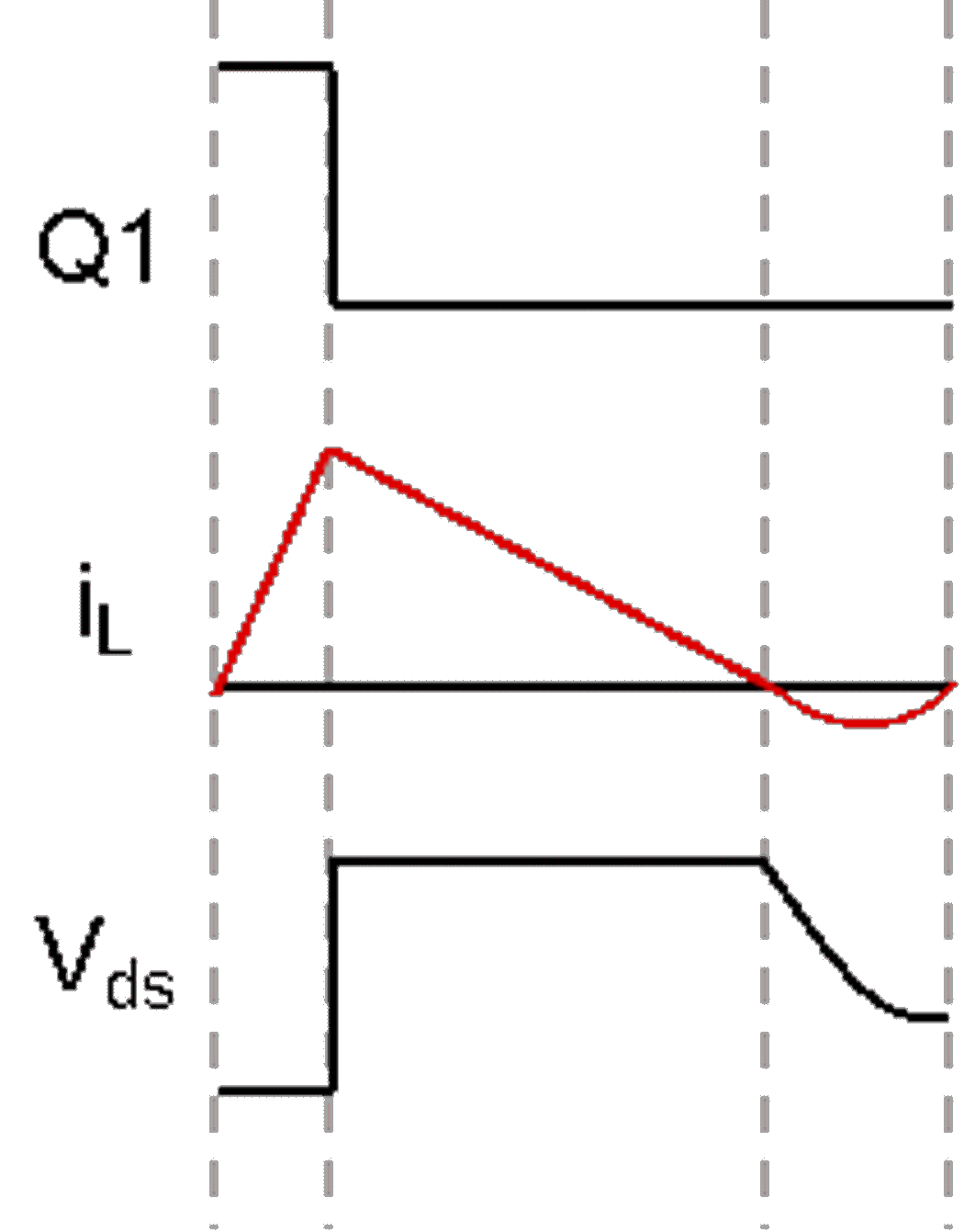
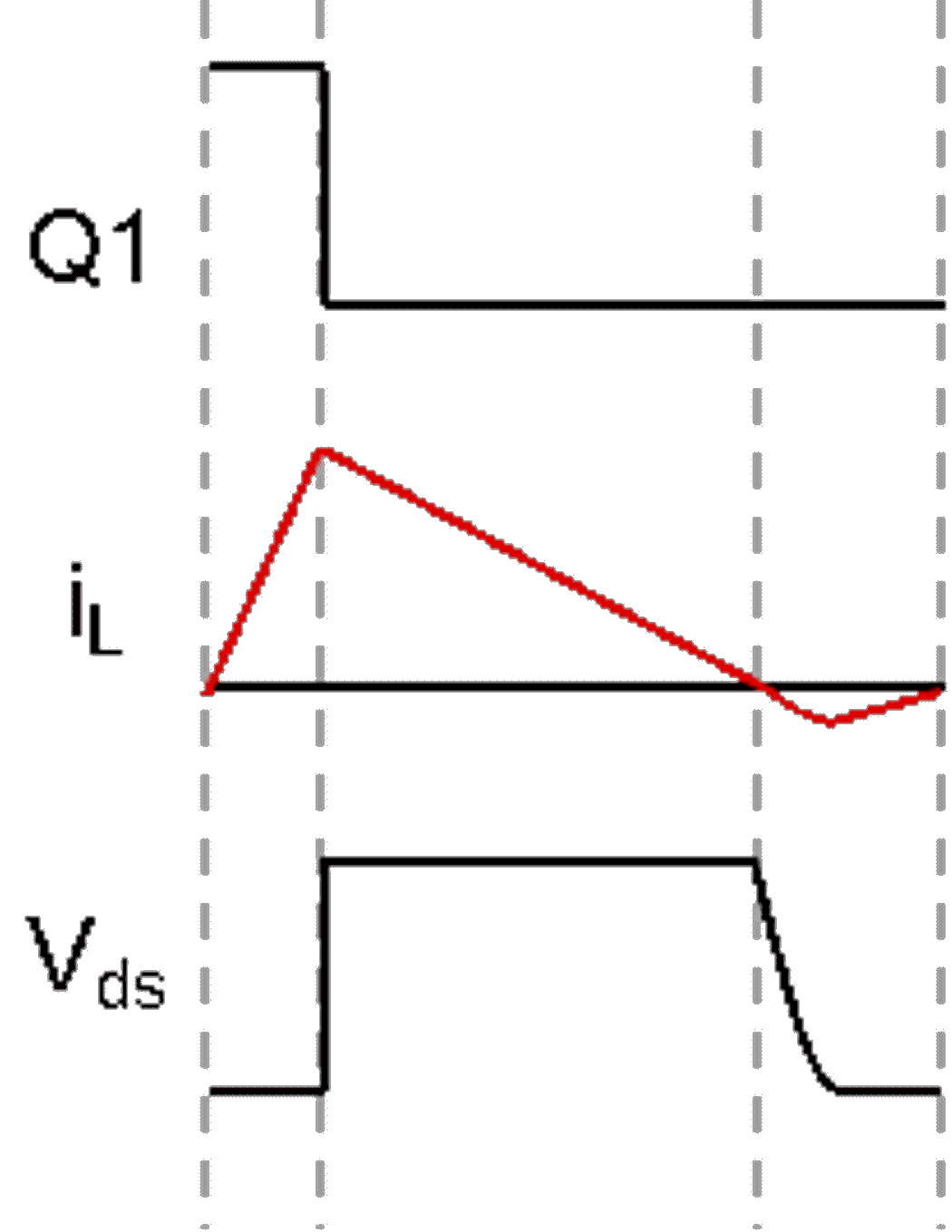
Figure 2-1 shows a conventional boost PFC topology. The inductor current iL can maintain the critical-conduction mode (CRM). When the inductor current become discontinuous, the MOSFET’s Vds voltage can resonate to zero and thereby create a ZVS switching instant. Figure 2 demonstrates PWM signal, MOSFET’s Vds and inductor current waveform in CRM/ZVS status.
 Figure 2-1 Boost PFC Topology
If AC input voltage is higher than half of DC bus voltage, the MOSFET should be turned ON at the valley point of the voltage to achieve ZCS(CRM). The MOSFET Vds never resonate to zero as shown in Figure 2-2. However, when AC input voltage is lower than 1/2 output voltage, the MOSFET’s Vds can resonate to zero volts and be clamped by the MOSFET body diode. MOSFET can achieve ZVS&ZCS in this status as shown in Figure 2-3.
 Figure 2-2 PFC Waveforms in CRM/ZVS Status:
Vin>Vout/2
 Figure 2-3 PFC Waveforms in CRM/ZVS Status:
Vin<Vout/2
Figure 2-3 PFC Waveforms in CRM/ZVS Status:
Vin<Vout/2The traditional predict-period approach requires fast calculation and consumes significant CPU bandwidth. The extra resource is used for calculating the resonant time and the duration that the boost inductor current iL return to zero from peak. This report proposes a MCU internal hardware-based method to realize CRM/ZVS PFC control by leveraging peripherals of C2000 MCU. These internal peripherals include CMPSS, cross bar (X-BAR) and type-4 PWM.