SPRACY9 March 2023 TMS320F2800132 , TMS320F2800132 , TMS320F2800133 , TMS320F2800133 , TMS320F2800135 , TMS320F2800135 , TMS320F2800137 , TMS320F2800137 , TMS320F2800152-Q1 , TMS320F2800152-Q1 , TMS320F2800153-Q1 , TMS320F2800153-Q1 , TMS320F2800154-Q1 , TMS320F2800154-Q1 , TMS320F2800155 , TMS320F2800155 , TMS320F2800155-Q1 , TMS320F2800155-Q1 , TMS320F2800156-Q1 , TMS320F2800156-Q1 , TMS320F2800157 , TMS320F2800157 , TMS320F2800157-Q1 , TMS320F2800157-Q1 , TMS320F280021 , TMS320F280021 , TMS320F280021-Q1 , TMS320F280021-Q1 , TMS320F280023 , TMS320F280023 , TMS320F280023-Q1 , TMS320F280023-Q1 , TMS320F280023C , TMS320F280023C , TMS320F280025 , TMS320F280025 , TMS320F280025-Q1 , TMS320F280025-Q1 , TMS320F280025C , TMS320F280025C , TMS320F280025C-Q1 , TMS320F280025C-Q1 , TMS320F280033 , TMS320F280033 , TMS320F280034 , TMS320F280034 , TMS320F280034-Q1 , TMS320F280034-Q1 , TMS320F280036-Q1 , TMS320F280036-Q1 , TMS320F280036C-Q1 , TMS320F280036C-Q1 , TMS320F280037 , TMS320F280037 , TMS320F280037-Q1 , TMS320F280037-Q1 , TMS320F280037C , TMS320F280037C , TMS320F280037C-Q1 , TMS320F280037C-Q1 , TMS320F280038-Q1 , TMS320F280038-Q1 , TMS320F280038C-Q1 , TMS320F280038C-Q1 , TMS320F280039 , TMS320F280039 , TMS320F280039-Q1 , TMS320F280039-Q1 , TMS320F280039C , TMS320F280039C , TMS320F280039C-Q1 , TMS320F280039C-Q1 , TMS320F280040-Q1 , TMS320F280040-Q1 , TMS320F280040C-Q1 , TMS320F280040C-Q1 , TMS320F280041 , TMS320F280041 , TMS320F280041-Q1 , TMS320F280041-Q1 , TMS320F280041C , TMS320F280041C , TMS320F280041C-Q1 , TMS320F280041C-Q1 , TMS320F280045 , TMS320F280045 , TMS320F280048-Q1 , TMS320F280048-Q1 , TMS320F280048C-Q1 , TMS320F280048C-Q1 , TMS320F280049 , TMS320F280049 , TMS320F280049-Q1 , TMS320F280049-Q1 , TMS320F280049C , TMS320F280049C , TMS320F280049C-Q1 , TMS320F280049C-Q1 , TMS320F28075 , TMS320F28075 , TMS320F28075-Q1 , TMS320F28075-Q1 , TMS320F28076 , TMS320F28076 , TMS320F28374D , TMS320F28374D , TMS320F28374S , TMS320F28374S , TMS320F28375D , TMS320F28375D , TMS320F28375S , TMS320F28375S , TMS320F28375S-Q1 , TMS320F28375S-Q1 , TMS320F28376D , TMS320F28376D , TMS320F28376S , TMS320F28376S , TMS320F28377D , TMS320F28377D , TMS320F28377D-EP , TMS320F28377D-EP , TMS320F28377D-Q1 , TMS320F28377D-Q1 , TMS320F28377S , TMS320F28377S , TMS320F28377S-Q1 , TMS320F28377S-Q1 , TMS320F28378D , TMS320F28378D , TMS320F28378S , TMS320F28378S , TMS320F28379D , TMS320F28379D , TMS320F28379D-Q1 , TMS320F28379D-Q1 , TMS320F28379S , TMS320F28379S , TMS320F28384D , TMS320F28384D , TMS320F28384D-Q1 , TMS320F28384D-Q1 , TMS320F28384S , TMS320F28384S , TMS320F28384S-Q1 , TMS320F28384S-Q1 , TMS320F28386D , TMS320F28386D , TMS320F28386D-Q1 , TMS320F28386D-Q1 , TMS320F28386S , TMS320F28386S , TMS320F28386S-Q1 , TMS320F28386S-Q1 , TMS320F28388D , TMS320F28388D , TMS320F28388S , TMS320F28388S , TMS320F28P650DH , TMS320F28P650DH , TMS320F28P650DK , TMS320F28P650DK , TMS320F28P650SH , TMS320F28P650SH , TMS320F28P650SK , TMS320F28P650SK , TMS320F28P659DK-Q1 , TMS320F28P659DK-Q1
- Abstract
- Trademarks
- 1Introduction
- 2Input Settling Design Steps
-
3Example Circuit Design
- 3.1 Select the ADC
- 3.2 Find the Minimum Op-Amp Bandwidth and RC Filter Ranges
- 3.3 Verify the Op-Amp Model
- 3.4 Build the ADC Input Model
- 3.5 Bias Point Analysis to Determine Voa_ss
- 3.6 Transient Analysis to Determine Voa_ss
- 3.7 Perform Initial Transient Analysis
- 3.8 Iterative Approach to Refine RC Filter Values
- 3.9 Perform Final Transient Analysis
- 3.10 Perform Final Transient Analysis
- 3.11 Further Refinement
- 3.12 Further Simulations
- 3.13 Completed Worksheet
- 4Working With Existing Circuits or Additional Constraints
- 5Summary
- 6References
3.9 Perform Final Transient Analysis
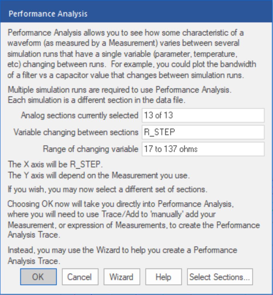
As an alternative to the iterative approach presented in Section 3.8, the Performance Analysis tool can be used to better select the optimal value of Rs. By applying the Performance Analysis tool to the initial sweep results presented in Figure 3-12, it is possible to graph settling error as a function of the value of Rs. To launch the Performance Analysis tool, go to Trace ➔ Performance Analysis... using the menu in the upper left of the PSpice for TI simulation window. The Performance Analysis tool is shown in Figure 3-15.
 Figure 3-15 F280049 Example Performance
Analysis
Figure 3-15 F280049 Example Performance
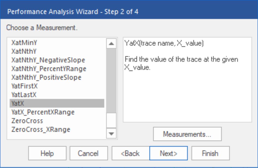
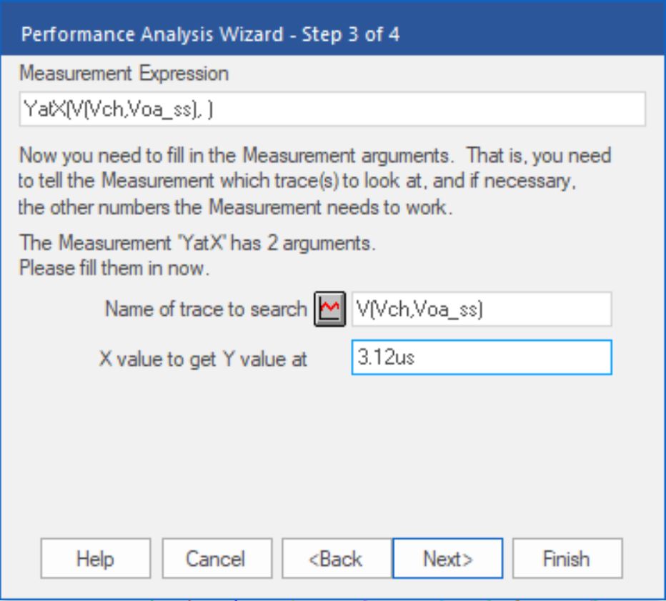
AnalysisUse the Wizard to create a Performance Analysis Trace. When prompted to choose a measurement, select YatX as shown in Figure 3-16. When prompted to complete the measurement expression, enter V(Vch, Voa_ss) as the name of the trace to search and 3.12 µs as the X value at which to measure the Y value as shown in Figure 3-17. Note that this measurement expression measures the Y value of the Verror trace at 3.12 µs, which is just past the end of an acquisition window. Thus, this measurement expression measures the settling error.
 Figure 3-16 F280049 Example Performance
Analysis Wizard - Step 2 of 4
 Figure 3-17 F280049 Example Performance
Analysis Wizard - Step 3 of 4
Figure 3-17 F280049 Example Performance
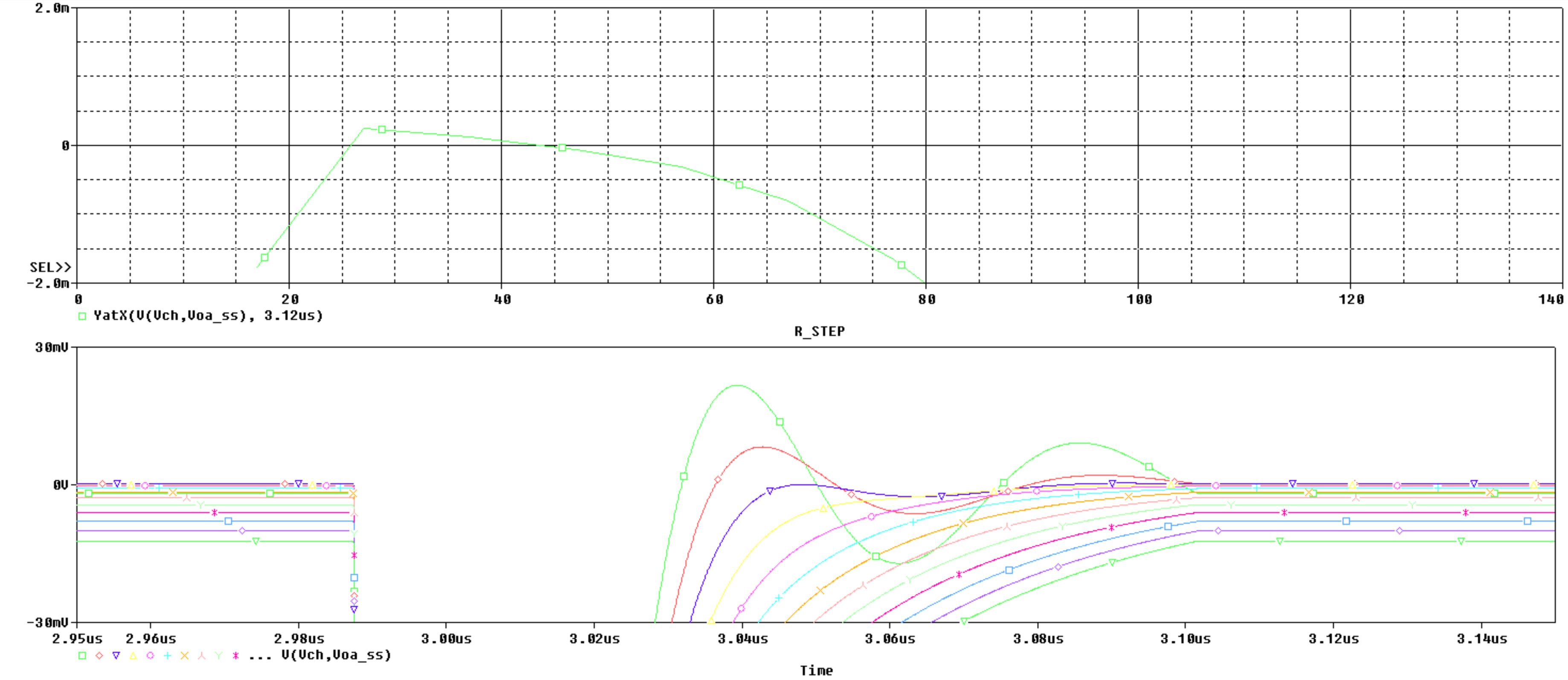
Analysis Wizard - Step 3 of 4When finished using the Wizard, a Performance Analysis Trace of settling error as a function of the value of Rs should appear as shown in Figure 3-18. Note that the settling error scale has been adjusted to show a range of -2 mV to +2 mV. The settling error scale can be further adjusted as desired by double-clicking on the vertical axis and modifying the Data Range.
 Figure 3-18 F280049 Example Performance
Analysis Trace
Figure 3-18 F280049 Example Performance
Analysis TraceExamining the Performance Analysis Trace shows that the settling error is approximately zero when the value of Rs is roughly 26 Ω and again when the value of Rs is roughly 44 Ω. However, Figure 3-12 shows that smaller values of Rs tend to result in greater oscillations of Verror than larger values of Rs. Greater oscillations of Verror are not ideal because small changes to the duration of the acquisition window can lead to large variations in settling error. Additionally, the slope of the Performance Analysis Trace at values of Rs near 26 Ω is steeper than the slope of the Performance Analysis Trace at values of Rs near 44 Ω. A steeper slope of the Performance Analysis Trace is not preferable because small variations in the value of Rs can lead to large changes in settling error. For this reason, values of Rs around 26 Ω are ignored in favor of values of Rs around 44 Ω.
Based on the Performance Analysis Trace, any value of Rs between 24 Ω and 56 Ω inclusive is expected to provide adequate settling. As a result, a final value of Rs can be selected from the set of standard resistor values in the range from 24 Ω to 56 Ω inclusive with a preference for standard resistor values near 44 Ω. The optimal value of Rs is the standard resistor value in this range that provides the least settling error. According to the Performance Analysis Trace, the 5% standard resistor value in this range that provides the least settling error is is 43 Ω. Thus, the final value of Rs is selected as the optimal value of 43 Ω.