SPRACY9 March 2023 F29H850TU , F29H850TU , F29H859TU-Q1 , F29H859TU-Q1 , TMS320F2800132 , TMS320F2800132 , TMS320F2800133 , TMS320F2800133 , TMS320F2800135 , TMS320F2800135 , TMS320F2800137 , TMS320F2800137 , TMS320F2800152-Q1 , TMS320F2800152-Q1 , TMS320F2800153-Q1 , TMS320F2800153-Q1 , TMS320F2800154-Q1 , TMS320F2800154-Q1 , TMS320F2800155 , TMS320F2800155 , TMS320F2800155-Q1 , TMS320F2800155-Q1 , TMS320F2800156-Q1 , TMS320F2800156-Q1 , TMS320F2800157 , TMS320F2800157 , TMS320F2800157-Q1 , TMS320F2800157-Q1 , TMS320F280021 , TMS320F280021 , TMS320F280021-Q1 , TMS320F280021-Q1 , TMS320F280023 , TMS320F280023 , TMS320F280023-Q1 , TMS320F280023-Q1 , TMS320F280023C , TMS320F280023C , TMS320F280025 , TMS320F280025 , TMS320F280025-Q1 , TMS320F280025-Q1 , TMS320F280025C , TMS320F280025C , TMS320F280025C-Q1 , TMS320F280025C-Q1 , TMS320F280033 , TMS320F280033 , TMS320F280034 , TMS320F280034 , TMS320F280034-Q1 , TMS320F280034-Q1 , TMS320F280036-Q1 , TMS320F280036-Q1 , TMS320F280036C-Q1 , TMS320F280036C-Q1 , TMS320F280037 , TMS320F280037 , TMS320F280037-Q1 , TMS320F280037-Q1 , TMS320F280037C , TMS320F280037C , TMS320F280037C-Q1 , TMS320F280037C-Q1 , TMS320F280038-Q1 , TMS320F280038-Q1 , TMS320F280038C-Q1 , TMS320F280038C-Q1 , TMS320F280039 , TMS320F280039 , TMS320F280039-Q1 , TMS320F280039-Q1 , TMS320F280039C , TMS320F280039C , TMS320F280039C-Q1 , TMS320F280039C-Q1 , TMS320F280040-Q1 , TMS320F280040-Q1 , TMS320F280040C-Q1 , TMS320F280040C-Q1 , TMS320F280041 , TMS320F280041 , TMS320F280041-Q1 , TMS320F280041-Q1 , TMS320F280041C , TMS320F280041C , TMS320F280041C-Q1 , TMS320F280041C-Q1 , TMS320F280045 , TMS320F280045 , TMS320F280048-Q1 , TMS320F280048-Q1 , TMS320F280048C-Q1 , TMS320F280048C-Q1 , TMS320F280049 , TMS320F280049 , TMS320F280049-Q1 , TMS320F280049-Q1 , TMS320F280049C , TMS320F280049C , TMS320F280049C-Q1 , TMS320F280049C-Q1 , TMS320F28075 , TMS320F28075 , TMS320F28075-Q1 , TMS320F28075-Q1 , TMS320F28076 , TMS320F28076 , TMS320F28374D , TMS320F28374D , TMS320F28374S , TMS320F28374S , TMS320F28375D , TMS320F28375D , TMS320F28375S , TMS320F28375S , TMS320F28375S-Q1 , TMS320F28375S-Q1 , TMS320F28376D , TMS320F28376D , TMS320F28376S , TMS320F28376S , TMS320F28377D , TMS320F28377D , TMS320F28377D-EP , TMS320F28377D-EP , TMS320F28377D-Q1 , TMS320F28377D-Q1 , TMS320F28377S , TMS320F28377S , TMS320F28377S-Q1 , TMS320F28377S-Q1 , TMS320F28378D , TMS320F28378D , TMS320F28378S , TMS320F28378S , TMS320F28379D , TMS320F28379D , TMS320F28379D-Q1 , TMS320F28379D-Q1 , TMS320F28379S , TMS320F28379S , TMS320F28384D , TMS320F28384D , TMS320F28384D-Q1 , TMS320F28384D-Q1 , TMS320F28384S , TMS320F28384S , TMS320F28384S-Q1 , TMS320F28384S-Q1 , TMS320F28386D , TMS320F28386D , TMS320F28386D-Q1 , TMS320F28386D-Q1 , TMS320F28386S , TMS320F28386S , TMS320F28386S-Q1 , TMS320F28386S-Q1 , TMS320F28388D , TMS320F28388D , TMS320F28388S , TMS320F28388S , TMS320F28P650DH , TMS320F28P650DH , TMS320F28P650DK , TMS320F28P650DK , TMS320F28P650SH , TMS320F28P650SH , TMS320F28P650SK , TMS320F28P650SK , TMS320F28P659DH-Q1 , TMS320F28P659DH-Q1 , TMS320F28P659DK-Q1 , TMS320F28P659DK-Q1 , TMS320F28P659SH-Q1 , TMS320F28P659SH-Q1
- Abstract
- Trademarks
- 1Introduction
- 2Input Settling Design Steps
-
3Example Circuit Design
- 3.1 Select the ADC
- 3.2 Find the Minimum Op-Amp Bandwidth and RC Filter Ranges
- 3.3 Verify the Op-Amp Model
- 3.4 Build the ADC Input Model
- 3.5 Bias Point Analysis to Determine Voa_ss
- 3.6 Transient Analysis to Determine Voa_ss
- 3.7 Perform Initial Transient Analysis
- 3.8 Iterative Approach to Refine RC Filter Values
- 3.9 Perform Final Transient Analysis
- 3.10 Perform Final Transient Analysis
- 3.11 Further Refinement
- 3.12 Further Simulations
- 3.13 Completed Worksheet
- 4Working With Existing Circuits or Additional Constraints
- 5Summary
- 6References
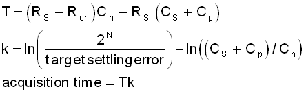
4.3.1 Analytical Solution for ADC Acquisition Time
A quick method for estimating the ADC S+H time given selections of Rs and Cs (along with the input model parameters from the device-specific data manual) is to use the formulas shown in Equation 1 and Equation 2: