SPRACZ9A November 2021 – December 2022 F28E120SC , TMS320F2800132 , TMS320F2800133 , TMS320F2800135 , TMS320F2800137 , TMS320F2800152-Q1 , TMS320F2800153-Q1 , TMS320F2800154-Q1 , TMS320F2800155 , TMS320F2800155-Q1 , TMS320F2800156-Q1 , TMS320F2800157 , TMS320F2800157-Q1 , TMS320F280021 , TMS320F280021-Q1 , TMS320F280023 , TMS320F280023-Q1 , TMS320F280023C , TMS320F280025 , TMS320F280025-Q1 , TMS320F280025C , TMS320F280025C-Q1 , TMS320F280033 , TMS320F280034 , TMS320F280034-Q1 , TMS320F280036-Q1 , TMS320F280036C-Q1 , TMS320F280037 , TMS320F280037-Q1 , TMS320F280037C , TMS320F280037C-Q1 , TMS320F280038-Q1 , TMS320F280038C-Q1 , TMS320F280039 , TMS320F280039-Q1 , TMS320F280039C , TMS320F280039C-Q1 , TMS320F280040-Q1 , TMS320F280040C-Q1 , TMS320F280041 , TMS320F280041-Q1 , TMS320F280041C , TMS320F280041C-Q1 , TMS320F280045 , TMS320F280048-Q1 , TMS320F280048C-Q1 , TMS320F280049 , TMS320F280049-Q1 , TMS320F280049C , TMS320F280049C-Q1
- Hardware Design Guide for F2800x Devices
- Trademarks
- 1Introduction
- 2Typical F2800x System Block Diagram
- 3Schematic Design
- 4PCB Layout Design
- 5EOS, EMI/EMC, and ESD Considerations
- 6Final Details and Checklist
- 7References
- 8Revision History
4.3 Placing Components
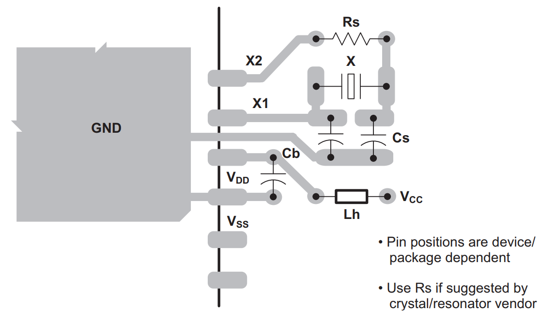
Once the position of the C2000 chip has been decided on the board, the next component that should be placed is the crystal/oscillator. This should be placed as close to the device as possible to ensure the most effective clocking solution. Specifically, traces to X1/X2 should remain as short as possible. Depending on the additional components required by the specific crystal being used, there are different ways in which a crystal/resonator can be routed on a board. Figure 4-4 is one example given a 2-layer board and a crystal that requires an additional series resistor Rs. When routing the clock traces from one device to another, try to use the 3W spacing rule. The distance from the center of the clock trace to the center of any adjacent signal trace should be at least three times the width of the clock trace. Many clocks, including slow frequency clocks, can have fast rise and fall times. Using the 3W rule cuts down on crosstalk between traces. In general, leave space between each of the traces running parallel between the devices. Avoid using right angles when routing traces to minimize the routing distance and impedance discontinuities. For further protection from crosstalk, run guard traces beside the clock signals (GND pin to GND pin), if possible. This lessens clock signal coupling.
 Figure 4-4 Recommended Oscillator Layout
The next most important components to place are the decoupling/bypass capacitors. These capacitors should be placed as close to their respective pins as possible and will further reduce noise and help ensure that the device’s power supplies are stable. Decoupling capacitors placed more than an inch away from the pins offer poor performance. Bulk capacitors, on the other hand, can be placed relatively further away from the chip without greatly impacting their performance. Figure 4-5 showcases good decoupling capacitor placement.
Other components that should follow are the JTAG header/circuitry and the XRSn circuitry.
For systems which make use of the internal 1.2 V DC-DC regulator on the TMS320F28004x device, the following outline key guidelines to ensure proper design of the DC-DC circuitry.
- TI recommends star-connecting VDDIO_SW and VDDIO to the same 3.3-V supply.
- All external components should be placed as close to the pins as possible.
- The loop formed by the VDDIO_SW, input capacitor (CVDDIO_SW), and VSS_SW must be as short as possible.
- The feedback trace must be as short as possible and kept away from any noise source such as the switching output (VSW).
- It is necessary to have a separate island or surgical cut in the ground plane for the input cap (CVDDIO_SW) and VSS_SW.
- A VDD plane is recommended for connecting the VDD node to the LVSW-CVDD point to minimize parasitic resistance and inductance.