SPRACZ9A November 2021 – December 2022 F28E120SC , TMS320F2800132 , TMS320F2800133 , TMS320F2800135 , TMS320F2800137 , TMS320F2800152-Q1 , TMS320F2800153-Q1 , TMS320F2800154-Q1 , TMS320F2800155 , TMS320F2800155-Q1 , TMS320F2800156-Q1 , TMS320F2800157 , TMS320F2800157-Q1 , TMS320F280021 , TMS320F280021-Q1 , TMS320F280023 , TMS320F280023-Q1 , TMS320F280023C , TMS320F280025 , TMS320F280025-Q1 , TMS320F280025C , TMS320F280025C-Q1 , TMS320F280033 , TMS320F280034 , TMS320F280034-Q1 , TMS320F280036-Q1 , TMS320F280036C-Q1 , TMS320F280037 , TMS320F280037-Q1 , TMS320F280037C , TMS320F280037C-Q1 , TMS320F280038-Q1 , TMS320F280038C-Q1 , TMS320F280039 , TMS320F280039-Q1 , TMS320F280039C , TMS320F280039C-Q1 , TMS320F280040-Q1 , TMS320F280040C-Q1 , TMS320F280041 , TMS320F280041-Q1 , TMS320F280041C , TMS320F280041C-Q1 , TMS320F280045 , TMS320F280048-Q1 , TMS320F280048C-Q1 , TMS320F280049 , TMS320F280049-Q1 , TMS320F280049C , TMS320F280049C-Q1
- Hardware Design Guide for F2800x Devices
- Trademarks
- 1Introduction
- 2Typical F2800x System Block Diagram
- 3Schematic Design
- 4PCB Layout Design
- 5EOS, EMI/EMC, and ESD Considerations
- 6Final Details and Checklist
- 7References
- 8Revision History
3.4.1 Power Requirements
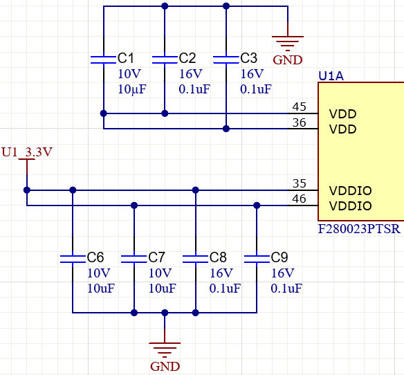
An important aspect in ensuring a robust and noise-resistant power supply to the device is including decoupling/bypass capacitors to ground for every power pin. These help to limit the spread of noise into other areas of the system, particularly to low-level analog signals. Decoupling capacitors minimize voltage drops/spikes on the power supply by acting as a filter and temporary energy storage, leading to a more stable power supply solution for the device.
 Figure 3-9 Decoupling Capacitors on VDD
Pins
Figure 3-9 Decoupling Capacitors on VDD
PinsWhen using an external voltage regulator (on supported devices) to power VDD, all VDD pins should be routed together to the same 1.2 V power rail. Decoupling capacitors are required on these pins to ensure stable voltage supplies. The value of this decoupling capacitor is device-dependent, so see the device-specific data sheet for the required value of CVDD. The VDDA and VDDIO power pins, likewise, also require decoupling capacitors to maintain a stable voltage supply. On all devices, all of the analog power pins (VDDA) should include a minimum 2.2 µF decoupling capacitor connected to analog ground (VSSA). The digital I/O power supply (VDDIO) requires a minimum 0.1 µF decoupling capacitor near each power pins, as shown in the figure above. For some devices, it is also recommended to place an additional bulk capacitor CVDDIO shared across all the pins. This bulk capacitance value is dependent on the regulator being used, so see the device-specific data sheet.
Of special note is the F28004x device, which contains an internal DC-DC regulator supply pin (VDDIO_SW). This pin should have a bulk input capacitance of 20 µF. The recommended configuration for this is two 10 µF capacitors in parallel. Additionally, this pin should be tied to the VDDIO pin and both pins must be supplied from the same 3.3 V source. If desired, a ferrite bead may be used for isolation.