SPRACZ9A November 2021 – December 2022 F28E120SC , TMS320F2800132 , TMS320F2800133 , TMS320F2800135 , TMS320F2800137 , TMS320F2800152-Q1 , TMS320F2800153-Q1 , TMS320F2800154-Q1 , TMS320F2800155 , TMS320F2800155-Q1 , TMS320F2800156-Q1 , TMS320F2800157 , TMS320F2800157-Q1 , TMS320F280021 , TMS320F280021-Q1 , TMS320F280023 , TMS320F280023-Q1 , TMS320F280023C , TMS320F280025 , TMS320F280025-Q1 , TMS320F280025C , TMS320F280025C-Q1 , TMS320F280033 , TMS320F280034 , TMS320F280034-Q1 , TMS320F280036-Q1 , TMS320F280036C-Q1 , TMS320F280037 , TMS320F280037-Q1 , TMS320F280037C , TMS320F280037C-Q1 , TMS320F280038-Q1 , TMS320F280038C-Q1 , TMS320F280039 , TMS320F280039-Q1 , TMS320F280039C , TMS320F280039C-Q1 , TMS320F280040-Q1 , TMS320F280040C-Q1 , TMS320F280041 , TMS320F280041-Q1 , TMS320F280041C , TMS320F280041C-Q1 , TMS320F280045 , TMS320F280048-Q1 , TMS320F280048C-Q1 , TMS320F280049 , TMS320F280049-Q1 , TMS320F280049C , TMS320F280049C-Q1
- Hardware Design Guide for F2800x Devices
- Trademarks
- 1Introduction
- 2Typical F2800x System Block Diagram
- 3Schematic Design
- 4PCB Layout Design
- 5EOS, EMI/EMC, and ESD Considerations
- 6Final Details and Checklist
- 7References
- 8Revision History
3.4.3.2 Internal LDO vs. Internal DC-DC Regulator
F28004x contains both an internal 1.2 V LDO voltage regulator (VREG) and an internal 1.2 V switching regulator (DC-DC). When implementing this device into a system, deciding between the internal LDO and the internal DC-DC solutions for the 1.2 V power rail is an important design decision when an external supply is not desired. The DC-DC regulator is significantly more efficient than the LDO, with the DC-DC regulator having 80% efficiency compared to the LDO regulator’s 30% efficiency. However, the DC-DC solution comes with a few trade-offs. Depending on the board layout, there is the potential for analog performance degradation, mostly impacting the ADC. Additionally, the DC-DC requires an external inductor and capacitors to function, leading to increased component cost. Finally, GPIO22 and will be occupied by VFBSW and GPIO23 by VSW, leading to reduced I/Os on the board. Overall, the DC-DC voltage regulator is useful for systems which require efficient voltage regulation and reduced noise (since its switching is external to the MCU) and where the additional component cost is not an issue.
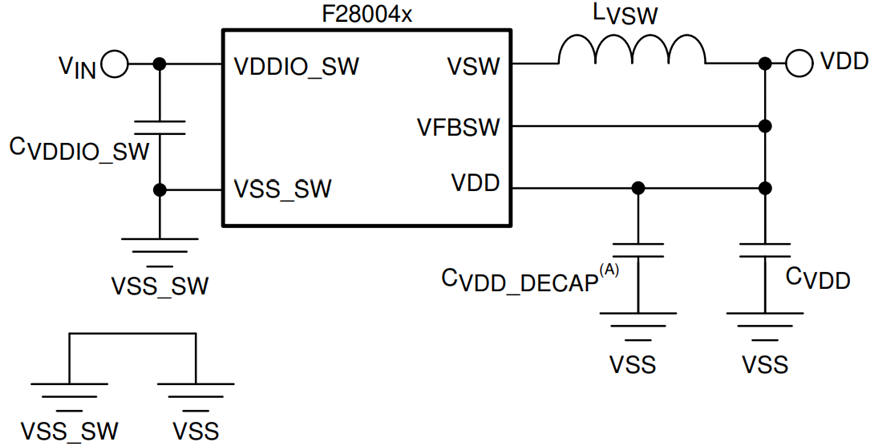
Figure 3-10 (also found in the TMS320F28004x Real-Time Microcontrollers Data Sheet) showcases the recommended design and required additional components when using the DC-DC regulator. Of special note is that an external connection should be made from the output of the internal DC-DC regulator to the VDD rail.
 Figure 3-10 DC-DC Regulator Circuit
Schematic