SPRACZ9A November 2021 – December 2022 F28E120SC , TMS320F2800132 , TMS320F2800133 , TMS320F2800135 , TMS320F2800137 , TMS320F2800152-Q1 , TMS320F2800153-Q1 , TMS320F2800154-Q1 , TMS320F2800155 , TMS320F2800155-Q1 , TMS320F2800156-Q1 , TMS320F2800157 , TMS320F2800157-Q1 , TMS320F280021 , TMS320F280021-Q1 , TMS320F280023 , TMS320F280023-Q1 , TMS320F280023C , TMS320F280025 , TMS320F280025-Q1 , TMS320F280025C , TMS320F280025C-Q1 , TMS320F280033 , TMS320F280034 , TMS320F280034-Q1 , TMS320F280036-Q1 , TMS320F280036C-Q1 , TMS320F280037 , TMS320F280037-Q1 , TMS320F280037C , TMS320F280037C-Q1 , TMS320F280038-Q1 , TMS320F280038C-Q1 , TMS320F280039 , TMS320F280039-Q1 , TMS320F280039C , TMS320F280039C-Q1 , TMS320F280040-Q1 , TMS320F280040C-Q1 , TMS320F280041 , TMS320F280041-Q1 , TMS320F280041C , TMS320F280041C-Q1 , TMS320F280045 , TMS320F280048-Q1 , TMS320F280048C-Q1 , TMS320F280049 , TMS320F280049-Q1 , TMS320F280049C , TMS320F280049C-Q1
- Hardware Design Guide for F2800x Devices
- Trademarks
- 1Introduction
- 2Typical F2800x System Block Diagram
- 3Schematic Design
- 4PCB Layout Design
- 5EOS, EMI/EMC, and ESD Considerations
- 6Final Details and Checklist
- 7References
- 8Revision History
4.1.3 Layer Stack-Up
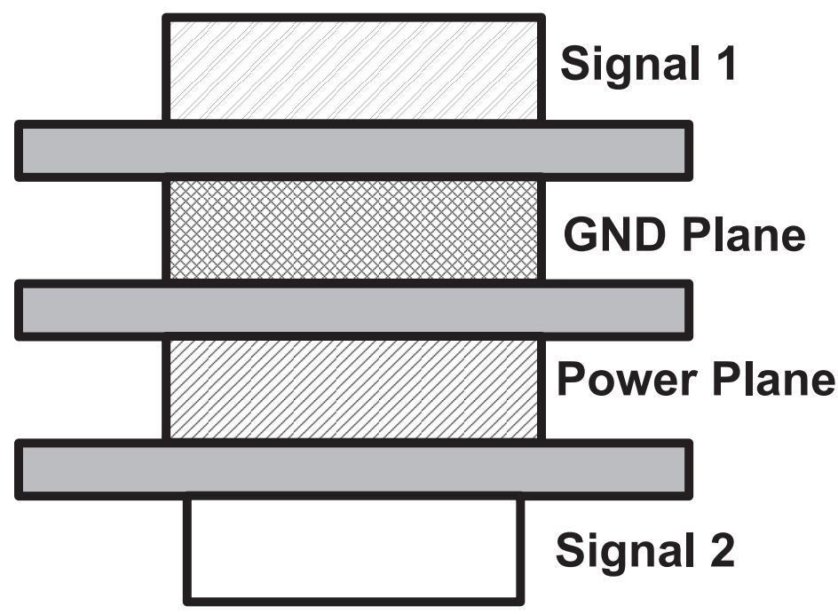
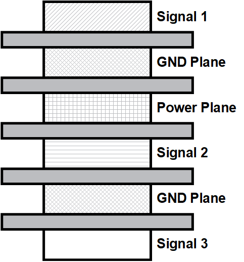
Choosing the number of board layers and the layer stack-up is dependent on the number of connections that need to be made on the PCB along with the cost of producing the PCB. A 4-layer board or more is often the best choice for C2000 devices. This enables the designer to include a clean ground plane and split power plane. In terms of configuration, two diagrams showcasing common 4-layer and 6-layer board stack-ups are shown. The 4-layer board stack-up consists of a signal/component layer, ground plane, split power plane (3.3 V, 1.2 V, and so forth), and signal/component layer. For the 6-layer board, the stack-up is as follows: signal/component layer, ground plane, split power plane (3.3 V, 1.2 V, and so forth), signal layer, another ground plane, and signal/component layer.
 Figure 4-1 Layer Stack-Up for 4-Layer
Board
 Figure 4-2 Layer Stack-Up for 6-Layer
Board