SPRACZ9A November 2021 – December 2022 F28E120SC , TMS320F2800132 , TMS320F2800133 , TMS320F2800135 , TMS320F2800137 , TMS320F2800152-Q1 , TMS320F2800153-Q1 , TMS320F2800154-Q1 , TMS320F2800155 , TMS320F2800155-Q1 , TMS320F2800156-Q1 , TMS320F2800157 , TMS320F2800157-Q1 , TMS320F280021 , TMS320F280021-Q1 , TMS320F280023 , TMS320F280023-Q1 , TMS320F280023C , TMS320F280025 , TMS320F280025-Q1 , TMS320F280025C , TMS320F280025C-Q1 , TMS320F280033 , TMS320F280034 , TMS320F280034-Q1 , TMS320F280036-Q1 , TMS320F280036C-Q1 , TMS320F280037 , TMS320F280037-Q1 , TMS320F280037C , TMS320F280037C-Q1 , TMS320F280038-Q1 , TMS320F280038C-Q1 , TMS320F280039 , TMS320F280039-Q1 , TMS320F280039C , TMS320F280039C-Q1 , TMS320F280040-Q1 , TMS320F280040C-Q1 , TMS320F280041 , TMS320F280041-Q1 , TMS320F280041C , TMS320F280041C-Q1 , TMS320F280045 , TMS320F280048-Q1 , TMS320F280048C-Q1 , TMS320F280049 , TMS320F280049-Q1 , TMS320F280049C , TMS320F280049C-Q1
- Hardware Design Guide for F2800x Devices
- Trademarks
- 1Introduction
- 2Typical F2800x System Block Diagram
- 3Schematic Design
- 4PCB Layout Design
- 5EOS, EMI/EMC, and ESD Considerations
- 6Final Details and Checklist
- 7References
- 8Revision History
3.5 XRSn and System Reset
Each of the F2800x devices contain a device reset (XRSn) pin that resets the device when driven low. This pin is also driven low upon power-on reset (POR), brownout reset (BOR), or watchdog reset. The internal POR circuit drives the XRSn and keeps all of the I/Os in a high-impedance state while the device is powering on. Once VDDIO crosses the POR threshold, control of the device is then given to the BOR. The BOR keeps holding the device in reset until VDDIO crosses the BOR threshold and arrives within the device’s operational range. Once this occurs, the device is no longer in reset and is functional. The BOR circuit itself is responsible for monitoring the VDDIO and checking that the supply rails remain within operational range. At any point during the operation of the device, if the VDDIO voltage drops below the BOR threshold, XRSn is pulled low and the device remains in reset until the voltage returns to the operational range. During the watchdog reset, the XRSn pin is driven low for the watchdog reset duration of 512 oscillator clock (OSCCLK) cycles.
Figure 3-11 showcases the device boot thresholds.
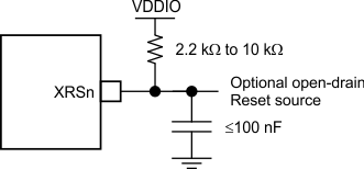
Apart from these internal reset circuits, a user may implement external circuitry that drives the XRSn pin and asserts a device reset. Note that this external circuitry should be done using an open-drain device. Examples of these outside circuits include external watchdogs, power management ICs, and voltage supervisors (for use in ASIL applications).
 Figure 3-12 External Reset Circuit
When designing the XRSn schematic, a strong pull-up resistor is required between the XRSn pin and VDDIO. This resistor should be between 2.2 kΩ and 10 kΩ in value. Furthermore, to improve noise filtering, a small capacitor is recommended between XRSn and VSS. This capacitor should be 100nF or less, as a larger capacitor will inhibit the ability of the watchdog reset to properly drive the XRSn pin. Due to significance of this pin, ESD protection diodes may also be added.