SPRACZ9A November 2021 – December 2022 F28E120SC , TMS320F2800132 , TMS320F2800133 , TMS320F2800135 , TMS320F2800137 , TMS320F2800152-Q1 , TMS320F2800153-Q1 , TMS320F2800154-Q1 , TMS320F2800155 , TMS320F2800155-Q1 , TMS320F2800156-Q1 , TMS320F2800157 , TMS320F2800157-Q1 , TMS320F280021 , TMS320F280021-Q1 , TMS320F280023 , TMS320F280023-Q1 , TMS320F280023C , TMS320F280025 , TMS320F280025-Q1 , TMS320F280025C , TMS320F280025C-Q1 , TMS320F280033 , TMS320F280034 , TMS320F280034-Q1 , TMS320F280036-Q1 , TMS320F280036C-Q1 , TMS320F280037 , TMS320F280037-Q1 , TMS320F280037C , TMS320F280037C-Q1 , TMS320F280038-Q1 , TMS320F280038C-Q1 , TMS320F280039 , TMS320F280039-Q1 , TMS320F280039C , TMS320F280039C-Q1 , TMS320F280040-Q1 , TMS320F280040C-Q1 , TMS320F280041 , TMS320F280041-Q1 , TMS320F280041C , TMS320F280041C-Q1 , TMS320F280045 , TMS320F280048-Q1 , TMS320F280048C-Q1 , TMS320F280049 , TMS320F280049-Q1 , TMS320F280049C , TMS320F280049C-Q1
- Hardware Design Guide for F2800x Devices
- Trademarks
- 1Introduction
- 2Typical F2800x System Block Diagram
- 3Schematic Design
- 4PCB Layout Design
- 5EOS, EMI/EMC, and ESD Considerations
- 6Final Details and Checklist
- 7References
- 8Revision History
3.1.3 PinMux Tool
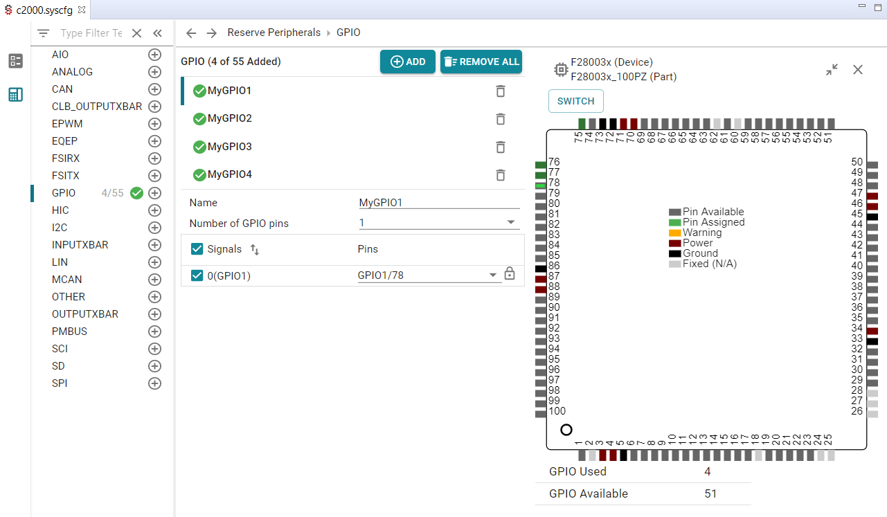
For a more streamlined pin assignment process, TI has developed a software tool known as the PinMux utility. This utility provides a graphical user interface for configuring pin multiplexing settings and resolving pin conflicts for C2000 devices. There is a deprecated standalone version of this software, but the most updated version can be found in TI’s SysConfig application. This tool, along with helping automate the pin configuration process, is a GUI that also aids in configuring peripherals, subsystems, and other components within TI’s devices. The SysConfig tool helps manage, expose, and resolve any device conflicts in real-time to ensure correct device configurations. The SysConfig tool can be found in three different forms: a standalone application, an integrated GUI within Code Composer Studio™, and an online cloud version.
 Figure 3-3 PinMux Tool Within
SysConfig