SPRACZ9A November 2021 – December 2022 F28E120SC , TMS320F2800132 , TMS320F2800133 , TMS320F2800135 , TMS320F2800137 , TMS320F2800152-Q1 , TMS320F2800153-Q1 , TMS320F2800154-Q1 , TMS320F2800155 , TMS320F2800155-Q1 , TMS320F2800156-Q1 , TMS320F2800157 , TMS320F2800157-Q1 , TMS320F280021 , TMS320F280021-Q1 , TMS320F280023 , TMS320F280023-Q1 , TMS320F280023C , TMS320F280025 , TMS320F280025-Q1 , TMS320F280025C , TMS320F280025C-Q1 , TMS320F280033 , TMS320F280034 , TMS320F280034-Q1 , TMS320F280036-Q1 , TMS320F280036C-Q1 , TMS320F280037 , TMS320F280037-Q1 , TMS320F280037C , TMS320F280037C-Q1 , TMS320F280038-Q1 , TMS320F280038C-Q1 , TMS320F280039 , TMS320F280039-Q1 , TMS320F280039C , TMS320F280039C-Q1 , TMS320F280040-Q1 , TMS320F280040C-Q1 , TMS320F280041 , TMS320F280041-Q1 , TMS320F280041C , TMS320F280041C-Q1 , TMS320F280045 , TMS320F280048-Q1 , TMS320F280048C-Q1 , TMS320F280049 , TMS320F280049-Q1 , TMS320F280049C , TMS320F280049C-Q1
- Hardware Design Guide for F2800x Devices
- Trademarks
- 1Introduction
- 2Typical F2800x System Block Diagram
- 3Schematic Design
- 4PCB Layout Design
- 5EOS, EMI/EMC, and ESD Considerations
- 6Final Details and Checklist
- 7References
- 8Revision History
4.4 Ground Plane
Copper planes on a PCB are excellent high-frequency capacitors and can be utilized for high-frequency bypassing along with the recommend capacitors. Another benefit of solid planes are that they can act as a good heat sink to mitigate excess thermal levels.
If the board has ample layers, a good practice is to place a ground place on the PCB. This ground plane not only assists in routing the ground signals on a board, but also helps in combating ground noise. Each signal on the board has a return current (via GND), and this ensures that the return path is through the path of least impedance. For boards with multiple ground planes on different layers, it is helpful to employ via stitching to connect these ground planes and further minimize impedance. For more information about return paths, see the Return Current and Loop Areas section of the High-Speed Layout Guidelines.
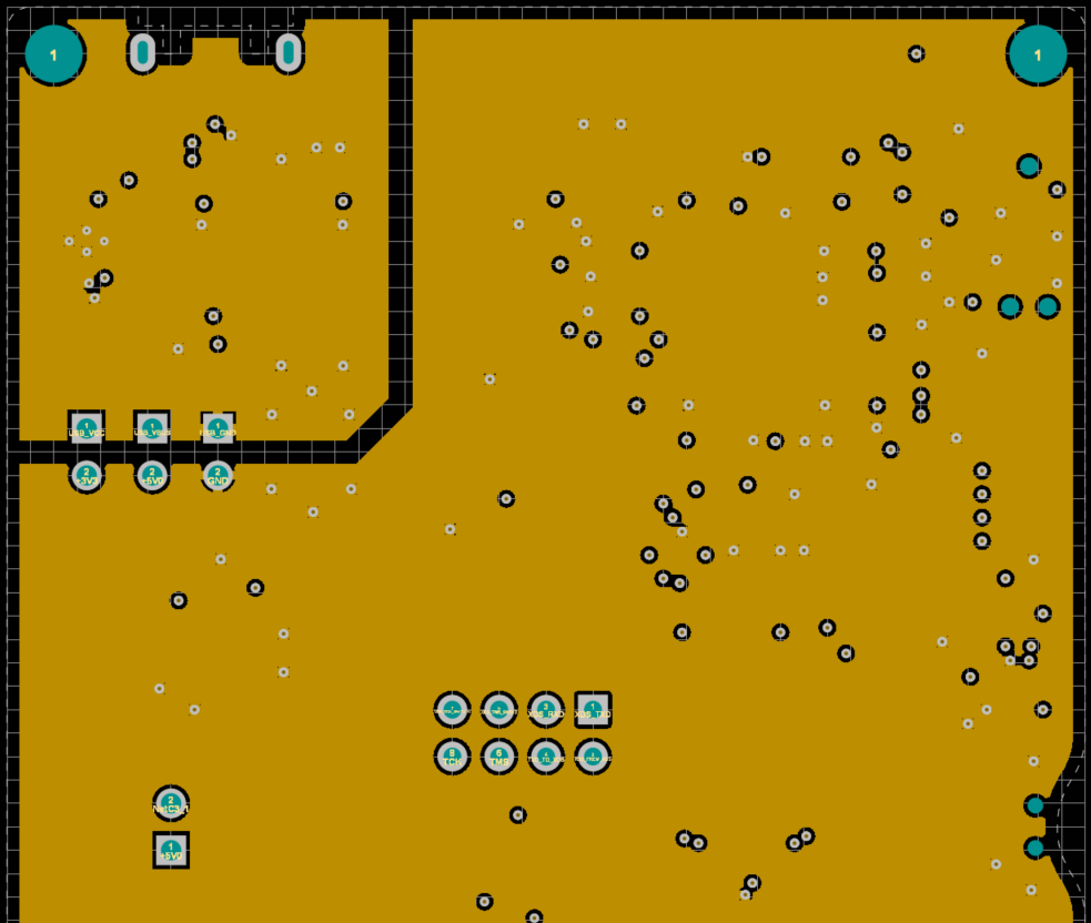
 Figure 4-7 Ground Plane on
LaunchPad
Figure 4-7 Ground Plane on
LaunchPadThe key to an effective ground plane is making sure that the plane remains intact and has good connections throughout the entire layer of the board. Onboard connections, such as vias and traces, can cut up the ground layer and reduce its effectiveness. Vias create a hole through multiple layers of the board and traces can sever the connection between different parts of the ground plane. In the left figure below, notice that the RGND vias only have a single connection to the ground plane and that the surrounding ground pore connections are very thin. Furthermore, in the Figure 4-8, notice that the top left of the pore is connected to the bottom left of the pour only through a thin sliver of copper. Both of these figures showcase undesirable ground planes. It would be helpful to rearrange the vias and traces to ensure that there are no thin ground plane connections or a severely cut-up ground pour.
When applying a ground plane to a layer, examine the plane to see if it has good connection throughout. Areas with missing planes or thin connections should be redesigned to maximize the ground plane area. Typically, this can be done by reducing the number of vias and by routing groups of traces closer to each other. In some cases, it may be helpful to modify the pinmux selection and schematic to improve routing. Sometimes these benefits may not be apparent until the layout routing process begins, but optimizing the pinmux can result in shorter trace lengths and reduced via usage, and thus a better ground plane.