SPRACZ9A November 2021 – December 2022 F28E120SC , TMS320F2800132 , TMS320F2800133 , TMS320F2800135 , TMS320F2800137 , TMS320F2800152-Q1 , TMS320F2800153-Q1 , TMS320F2800154-Q1 , TMS320F2800155 , TMS320F2800155-Q1 , TMS320F2800156-Q1 , TMS320F2800157 , TMS320F2800157-Q1 , TMS320F280021 , TMS320F280021-Q1 , TMS320F280023 , TMS320F280023-Q1 , TMS320F280023C , TMS320F280025 , TMS320F280025-Q1 , TMS320F280025C , TMS320F280025C-Q1 , TMS320F280033 , TMS320F280034 , TMS320F280034-Q1 , TMS320F280036-Q1 , TMS320F280036C-Q1 , TMS320F280037 , TMS320F280037-Q1 , TMS320F280037C , TMS320F280037C-Q1 , TMS320F280038-Q1 , TMS320F280038C-Q1 , TMS320F280039 , TMS320F280039-Q1 , TMS320F280039C , TMS320F280039C-Q1 , TMS320F280040-Q1 , TMS320F280040C-Q1 , TMS320F280041 , TMS320F280041-Q1 , TMS320F280041C , TMS320F280041C-Q1 , TMS320F280045 , TMS320F280048-Q1 , TMS320F280048C-Q1 , TMS320F280049 , TMS320F280049-Q1 , TMS320F280049C , TMS320F280049C-Q1
- Hardware Design Guide for F2800x Devices
- Trademarks
- 1Introduction
- 2Typical F2800x System Block Diagram
- 3Schematic Design
- 4PCB Layout Design
- 5EOS, EMI/EMC, and ESD Considerations
- 6Final Details and Checklist
- 7References
- 8Revision History
3.7.1 JTAG/cJTAG
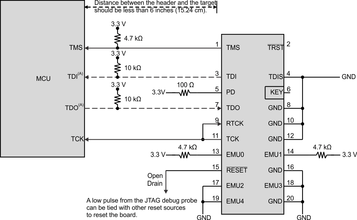
The F2800x devices feature a JTAG port with four dedicated pins: TMS, TCK, TDI, and TDO. These correspond to test-mode select, test clock, test data input, and test data output. An external 2.2 kΩ pull-up resistor on the board should tie the TMS pin to VDDIO to keep JTAG in reset during normal operation. There is also a cJTAG (IEEE Standard 1149.7) port, which is a compact 2-pin JTAG interface that only features TMS and TCK. When using cJTAG, other device functionality can be muxed to the traditional GPIO35 (TDI) and GPIO37 (TDO) pins to allow for full emulation and debugging capabilities.
When choosing between JTAG and cJTAG, consider the system requirements in terms of interface speed, debug functionality, and pin constraints. JTAG should be used if interface speed is of great importance, as JTAG is around 2-3 times faster than cJTAG. Additionally, using JTAG also enables the ability to daisy-chain multiple devices on a single JTAG header. cJTAG should be used if pin usage is constrained, as using cJTAG frees up 2 GPIO pins on the device. Apart from the performance drawback, the TMS pin is bidirectional when cJTAG is used, which could impact isolation strategies. Overall, if pins usage is not constrained, normal JTAG is recommended because of its performance advantages.
Although JTAG debug probes are included in all C2000 evaluation modules, TI does not recommend including the JTAG debug probe directly on the board. All EVMs include these headers to allow for streamlined debugging and emulation as well as the ability to use the EVM as a standalone debug probe. In actual C2000 applications, an on-board debug probe is not necessary and adds additional costs. Instead, if JTAG functionality is desired, it is recommended to include a JTAG header for connecting to an external probe. In instances where the MCU target and the JTAG header are farther than 6 inches (15.24 cm) apart or other devices are present on the JTAG chain, then each JTAG signal should be buffered.
 Figure 3-16 Typical JTAG Probe
Connections
Figure 3-16 Typical JTAG Probe
ConnectionsFor even more information about using JTAG with C2000 devices, see the C2000 MCU JTAG Connectivity Debug.