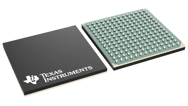
Packaging information
| Package | Pins NFBGA (NZH) | 196 |
| Operating temperature range (°C) -40 to 85 |
| Package qty | Carrier 119 | JEDEC TRAY (10+1) |
Features for the DS92LV1260
- Deserializes One to Six BusLVDS Input Serial Data Streams with Embedded Clocks
- Seven Selectable Serial Inputs to Support n+1 Redundancy of Deserialized Streams
- Seventh Channel has Single Pin Monitor Output That Reflects Input From Seventh Channel Input
- Parallel Clock Rate up to 40MHz
- On Chip Filtering for PLL
- Absolute Maximum Worst Case Power Dissipation = 1.9W at 3.6V
- High Impedance Inputs Upon Power Off (Vcc = 0V)
- Single Power Supply at +3.3V
- 196-pin NFBGA Package (Low-profile Ball Grid Array) Package
- Industrial Temperature Range Operation: −40°C to +85°C
All trademarks are the property of their respective owners.
Description for the DS92LV1260
The DS92LV1260 integrates six deserializer devices into a single chip. The chip uses a 0.25u CMOS process technology. The DS92LV1260 can simultaneously deserialize up to six data streams that have been serialized by the Texas Instruments DS92LV1021 or DS92LV1023 Bus LVDS serializers. The device also includes a seventh serial input channel that serves as a redundant input.
Each deserializer block in the DS92LV1260 operates independently with its own clock recovery circuitry and lock-detect signaling.
The DS92LV1260 uses a single +3.3V power supply with a typical power dissipation of 1.2W at 3.3V with a PRBS-15 pattern. Refer to the Connection Diagrams for packaging information.