인터페이스 LVDS, M-LVDS 및 PECL IC

SN55LVRA4-SEP

활성

쿼드 채널 고속 차동 리시버

제품 상세 정보

Function Receiver Protocols LVDS Number of transmitters 0 Number of receivers 4 Supply voltage (V) 3.3 Signaling rate (Mbps) 400 Input signal CMOS, ECL, LVCMOS, LVDS, LVECL, LVPECL, PECL Output signal LVTTL Rating Space Operating temperature range (°C) -55 to 125
SOIC (D) 16 59.4 mm² 9.9 x 6
  • VID V62/25606-01XE
  • Total ionizing dose characterized at 30krad (Si)
    • Total ionizing dose radiation lot acceptance testing (TID RLAT) for every wafer lot to 30krad (Si)
  • Single-event effects (SEE) characterized:
    • Single event latch-up (SEL) immune to linear energy transfer (LET) = 50MeV-cm2 /mg
    • Single event transient (SET) characterization report available
  • 400Mbps signaling rate
  • Operates with a single 3.3V supply
  • –4V to 5V extended common-mode input voltage range
  • Differential input thresholds < ±50mV with 50mV of hysteresis over entire common-mode input voltage range
  • Complies with TIA/EIA-644 (LVDS)
  • Active fail-safe assures a high-level output with no input and input remains high-impedance on power down
  • Bus-pin ESD protection exceeds 15kV HBM
  • TTL control inputs are 5V tolerant
  • Space enhanced plastic (SEP)
    • Controlled baseline
    • Gold wire, NiPdAu lead finish
    • One assembly and test site, one fabrication site
    • Extended product life cycle
    • Military (–55°C to 125°C) temperature range
    • Product traceability
    • Meets NASA ASTM E595 outgassing specification

The SN55LVRA4-SEP offers the widest common-mode input voltage range in the industry. These receivers provide an input voltage range specification compatible with a 5V PECL signal as well as an overall increased ground-noise tolerance.

The SN55LVRA4-SEP include a failsafe circuit that provides a high-level output within 60ns after loss of the input signal. The most common causes of signal loss are disconnected cables, shorted lines, or powered-down transmitters. The failsafe circuit prevents noise from being received as valid data under these fault conditions.

The intended application and signaling technique of these devices is point-to-point baseband data transmission over controlled impedance media of approximately 100Ω. The transmission media can be printed-circuit board traces, backplanes, or cables. The ultimate rate and distance of data transfer is dependent upon the attenuation characteristics of the media and the noise coupling to the environment.

The SN55LVRA4-SEP is characterized for operation from –55°C to 125°C.

다운로드 스크립트와 함께 비디오 보기 동영상

관심 가지실만한 유사 제품

open-in-new 대안 비교
비교 대상 장치와 유사한 기능
신규 SN55LVTA4-SEP 활성 방사선 내성 쿼드 채널 고속 차동 라인 드라이버 Line Driver version

기술 자료

star =TI에서 선정한 이 제품의 인기 문서
검색된 결과가 없습니다. 검색어를 지우고 다시 시도하십시오.
5개 모두 보기
유형 직함 날짜
* Data sheet SN55LVRA4-SEP Radiation Tolerant Quad Channel High-Speed Differential Receiver datasheet (Rev. A) PDF | HTML 2025/12/05
* Radiation & reliability report SN55LVRA4-SEP Total Ionizing Dose (TID) Report 2025/12/10
* Radiation & reliability report SN55LVRA4-SEP Single-Event Effects (SEE) Radiation Report PDF | HTML 2025/12/08
* Radiation & reliability report SN55LVRA4-SEP Production Flow and Reliability Report PDF | HTML 2025/11/12
Selection guide TI Space Products (Rev. K) 2025/04/04

설계 및 개발

추가 조건 또는 필수 리소스는 사용 가능한 경우 아래 제목을 클릭하여 세부 정보 페이지를 확인하세요.

평가 보드

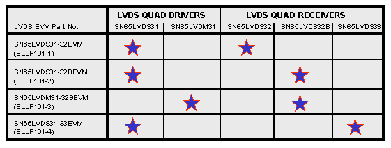
SN65LVDS31-33EVM — SN65LVDS31 및 SN65LVDS33용 평가 모듈

TI offers a series of low-voltage differential signaling (LVDS) evaluation modules (EVMs) designed for analysis of the electrical characteristics of LVDS drivers and receivers. Four unique EVMs are available to evaluate the different classes of LVDS devices offered by TI.

As seen in the Combination (...)

사용 설명서: PDF
TI.com에서 구매 불가
시뮬레이션 모델

SN65LVDS33 IBIS Model (Rev. A)

SLLC069A.ZIP (6 KB) - IBIS Model
시뮬레이션 툴

PSPICE-FOR-TI — TI 설계 및 시뮬레이션 툴용 PSpice®

TI용 PSpice®는 아날로그 회로의 기능을 평가하는 데 사용되는 설계 및 시뮬레이션 환경입니다. 완전한 기능을 갖춘 이 설계 및 시뮬레이션 제품군은 Cadence®의 아날로그 분석 엔진을 사용합니다. 무료로 제공되는 TI용 PSpice에는 아날로그 및 전력 포트폴리오뿐 아니라 아날로그 행동 모델에 이르기까지 업계에서 가장 방대한 모델 라이브러리 중 하나가 포함되어 있습니다.

TI 설계 및 시뮬레이션 환경용 PSpice는 기본 제공 라이브러리를 이용해 복잡한 혼합 신호 설계를 시뮬레이션할 수 있습니다. 레이아웃 및 제작에 착수하기 (...)
시뮬레이션 툴

TINA-TI — SPICE 기반 아날로그 시뮬레이션 프로그램

TINA-TI provides all the conventional DC, transient and frequency domain analysis of SPICE and much more. TINA has extensive post-processing capability that allows you to format results the way you want them. Virtual instruments allow you to select input waveforms and probe circuit nodes voltages (...)
사용 설명서: PDF
패키지 CAD 기호, 풋프린트 및 3D 모델
SOIC (D) 16 Ultra Librarian

주문 및 품질

포함된 정보:
  • RoHS
  • REACH
  • 디바이스 마킹
  • 납 마감/볼 재질
  • MSL 등급/피크 리플로우
  • MTBF/FIT 예측
  • 물질 성분
  • 인증 요약
  • 지속적인 신뢰성 모니터링
포함된 정보:
  • 팹 위치
  • 조립 위치

권장 제품에는 본 TI 제품과 관련된 매개 변수, 평가 모듈 또는 레퍼런스 디자인이 있을 수 있습니다.

지원 및 교육

TI 엔지니어의 기술 지원을 받을 수 있는 TI E2E™ 포럼

콘텐츠는 TI 및 커뮤니티 기고자에 의해 "있는 그대로" 제공되며 TI의 사양으로 간주되지 않습니다. 사용 약관을 참조하십시오.

품질, 패키징, TI에서 주문하는 데 대한 질문이 있다면 TI 지원을 방문하세요. ​​​​​​​​​​​​​​

동영상