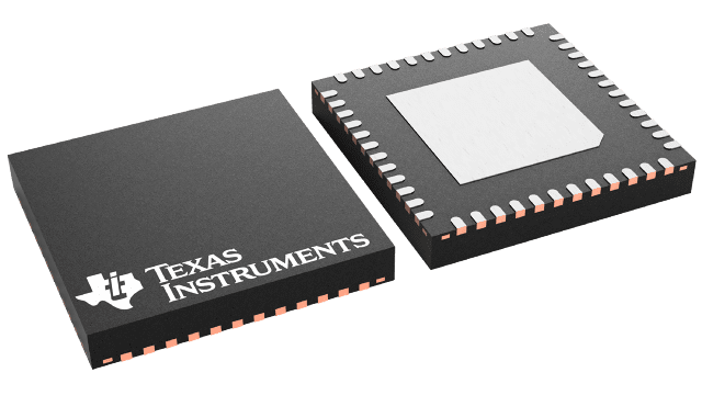
Packaging information
| Package | Pins VQFN (RGZ) | 48 |
| Operating temperature range (°C) -40 to 85 |
| Package qty | Carrier 2,500 | LARGE T&R |
Features for the SN65LVCP204
- Up to 2.5-Gbps Operation
- Non-Blocking Architecture Allows Each
Output to Be Connected to Any Input - 30 ps of Deterministic Jitter
- Selectable Transmit Preemphasis Per Lane
- Selectable Receive Equalization
- Available Packaging: 48-Pin QFN
- Propagation Delay Times: 500 ps Typical
- Inputs Electrically Compatible With
CML Signal Levels - Operates From a Single 3.3-V Supply
- Ability to Place Ouputs in High-Impedance State
- Low Power: 560 mW
- Integrated Termination Resistors
- APPLICATIONS
- Clock Buffering/Clock MUXing
- Wireless Base Stations
- High-Speed Network Routing
- Telecom/Datacom
Description for the SN65LVCP204
The SN65LVCP204 is a 4×4 non-blocking crosspoint switch in a flow-through pinout that allows for ease in PCB layout. VML signaling is used to achieve a high-speed data throughput while using low power. Each of the output drivers includes a 4:1 multiplexer to allow any input to be routed to any output. Internal signal paths are fully differential to achieve high signaling speeds while maintaining low signal skews. The SN65LVCP204 incorporates 100- termination resistors for those applications where board space is at a premium. Transmit preemphasis and receive equalization are built in for superior signal integrity performance.