SBOS487B June 2009 – March 2020 PGA280
PRODUCTION DATA.
- 1 Features
- 2 Applications
- 3 Description
- 4 Revision History
- 5 Pin Configuration and Functions
- 6 Specifications
-
7 Detailed Description
- 7.1 Overview
- 7.2 Functional Block Diagram
- 7.3 Feature Description
- 7.4 Device Functional Modes
- 7.5 Programming
- 7.6
Register Map
- 7.6.1 Register 0: Gain and External MUX Address (address = 00h) [reset = 0000 0000b]
- 7.6.2 Register 1: Software Reset Register (address = 01h) [reset = 0000 0000b]
- 7.6.3 Register 2: SPI: MODE Selection to GPIO-Pin (address = 02h) [reset = 0000 0000b]
- 7.6.4 Register 3: BUF Timeout Register (address = 03h) [reset = 0001 1001b]
- 7.6.5 Register 4: Error Register (address = 04h) [reset = 0000 0000b]
- 7.6.6 Register 5: GPIO Register (address = 05h) [reset = 0000 0000b]
- 7.6.7 Register 6: Input Switch Control Register 1 (address = 06h) [reset = 0110 0000b]
- 7.6.8 Register 7: Input Switch Control Register 2 (address =07h ) [reset = 0000 0000b]
- 7.6.9 Register 8: GPIO Configuration Register (address = 08h) [reset = 0000 0000b]
- 7.6.10 Register 9: CS Configuration Mode Register (address = 09h) [reset = 0000 0000b]
- 7.6.11 Register 10: Configuration Register 1 (address = 0Ah) [reset = 0000 0000b]
- 7.6.12 Register 11: Configuration Register 2 (address = 0Bh) [reset = 0001 0000b]
- 7.6.13 Register 12: Special Functions Register (address = 0Ch) [reset = 0000 0000b]
- 8 Application and Implementation
- 9 Power Supply Recommendations
- 10Device and Documentation Support
- 11Mechanical, Packaging, and Orderable Information
Package Options
Mechanical Data (Package|Pins)
- PW|24
Thermal pad, mechanical data (Package|Pins)
Orderable Information
7.3.1.1 Input Switch Network
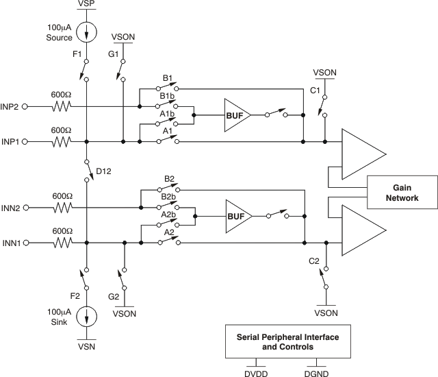
Figure 44 shows the arrangement of the input switches. They are controlled individually via the digital SPI. The switches B1b, B2b, A1b, and A2b are controlled automatically with the buffer (BUF) operation.
 Figure 44. Input Switch Diagram
 Switches A and B select the signal input. Input 1 (INP1 and INN1) provides two current sources and two switches that connect to VSON (which is typically the analog ground). This configuration is intended for wire break diagnosis. D12 can discharge an external capacitor or generate a starting condition.
Switches C1 and C2 are used to measure the input voltage referred to GND (VSON); for example, with A1 and C2 closed. This scheme measures the voltage signal connected to the input pin (INP1) referred to a common ground. The BUF output is protected against a short to VSON. See the section for more information about switch control.