SBOS487B June 2009 – March 2020 PGA280
PRODUCTION DATA.
- 1 Features
- 2 Applications
- 3 Description
- 4 Revision History
- 5 Pin Configuration and Functions
- 6 Specifications
-
7 Detailed Description
- 7.1 Overview
- 7.2 Functional Block Diagram
- 7.3 Feature Description
- 7.4 Device Functional Modes
- 7.5 Programming
- 7.6
Register Map
- 7.6.1 Register 0: Gain and External MUX Address (address = 00h) [reset = 0000 0000b]
- 7.6.2 Register 1: Software Reset Register (address = 01h) [reset = 0000 0000b]
- 7.6.3 Register 2: SPI: MODE Selection to GPIO-Pin (address = 02h) [reset = 0000 0000b]
- 7.6.4 Register 3: BUF Timeout Register (address = 03h) [reset = 0001 1001b]
- 7.6.5 Register 4: Error Register (address = 04h) [reset = 0000 0000b]
- 7.6.6 Register 5: GPIO Register (address = 05h) [reset = 0000 0000b]
- 7.6.7 Register 6: Input Switch Control Register 1 (address = 06h) [reset = 0110 0000b]
- 7.6.8 Register 7: Input Switch Control Register 2 (address =07h ) [reset = 0000 0000b]
- 7.6.9 Register 8: GPIO Configuration Register (address = 08h) [reset = 0000 0000b]
- 7.6.10 Register 9: CS Configuration Mode Register (address = 09h) [reset = 0000 0000b]
- 7.6.11 Register 10: Configuration Register 1 (address = 0Ah) [reset = 0000 0000b]
- 7.6.12 Register 11: Configuration Register 2 (address = 0Bh) [reset = 0001 0000b]
- 7.6.13 Register 12: Special Functions Register (address = 0Ch) [reset = 0000 0000b]
- 8 Application and Implementation
- 9 Power Supply Recommendations
- 10Device and Documentation Support
- 11Mechanical, Packaging, and Orderable Information
Package Options
Mechanical Data (Package|Pins)
- PW|24
Thermal pad, mechanical data (Package|Pins)
Orderable Information
7.3.1.3 Current Buffer
Designed for highest accuracy and low noise, both amplifier inputs are protected from dynamic overvoltages through clamps. The amplifier fast input slew rate (approximately 1 V/µs) normally prevents these clamps from turning on, provided adequate signal filtering is placed before the input. However, the fast channel switching-transient of a multiplexer or switch is much steeper, and cannot be filtered; this type of transient generates a dynamic overload. The current buffers (BUF) prevent this dynamic overload condition of the input.
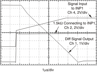
With the buffers not activated, Figure 45 indicates the clamp current flowing as a result of a fast signal change. The ramp in the signal, measured at the input pins (INP1), is the resulting voltage drop across the 1.5-kΩ resistor. In the example measurement, this resistor is placed between the signal generator and the input pin of the PGA280.
 Figure 45. Buffer OFF: Input Clamp Current Flowing
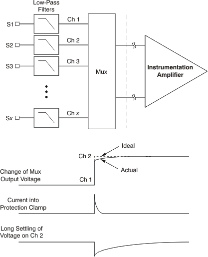
 Figure 46 shows a typical block diagram for multiplexed data acquisition. The transient from channel 1 to channel 2 , shown as a voltage step, dynamically overloads the amplifier. A current pulse results from the input protection clamp. Without the activation of the buffers (see BUF, Figure 44), the clamp current charges the filter and the signal source. Input low-pass filters are often set to settling times in the millisecond range; therefore, discharge currents from dynamic overload would produce long settling delays.

NOTE:
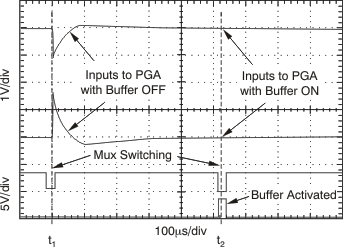
Current from the protection clamp into the signal source and filter produces a long settling delay.Together with the switching command of the multiplexer or internal switching, the current buffers (BUF) can be activated to prevent such clamp currents. The buffers do not have clamps as long as the signal remains within the supply boundaries. Figure 47 shows an example of the input signal settling for both conditions: without and with the buffer activated.
Without the buffer, there is an obvious long settling, depending on signal and filter impedance. With the buffer activated, only the amplifier has to settle and no distorting current is reflected into the signal source and filter; no glitch is visible in this plot. The plot shows the resulting settling of the input signal for a positive and a negative signal step as indicated in Figure 46; also shown are the SPI signal and the BUFA signal.
 Figure 47. Example for Amplifier Settling Without (t1) and With (t2) Buffer (BUF) Activated
 The buffers turn off automatically after a preset time (see Register 3, BUFTIM). They are activated from bit 5 (T) within the command byte. They can also be triggered by an external pin (BUFTin on GPIO4). The BUFA bit is active in conjunction with the buffer, indicating that the buffer is busy (see Figure 55).
Error detection circuits observe the signal path for signal overvoltage (IOVerr), amplifier output clipping (IARerr), and gain overload (GAINerr). The Input Clamp Activation indicator ICAerr indicates that current was conducted into the dynamic clamp circuit. These indicators help prevent misinterpretation of the analog signal and diagnose critical input signal conditions, such as those that occur with integrating analog-to-digital converters that may hide momentary overloads and present inaccurate results.
The buffers (BUF) prevent current flowing from the signal source with a compromise of offset voltage. As soon as the buffers are turned off, the amplifiers settle back to high precision. For signal measurement without (multiplexer) switching transients, the buffer is not used.