SBOS487B June 2009 – March 2020 PGA280
PRODUCTION DATA.
- 1 Features
- 2 Applications
- 3 Description
- 4 Revision History
- 5 Pin Configuration and Functions
- 6 Specifications
-
7 Detailed Description
- 7.1 Overview
- 7.2 Functional Block Diagram
- 7.3 Feature Description
- 7.4 Device Functional Modes
- 7.5 Programming
- 7.6
Register Map
- 7.6.1 Register 0: Gain and External MUX Address (address = 00h) [reset = 0000 0000b]
- 7.6.2 Register 1: Software Reset Register (address = 01h) [reset = 0000 0000b]
- 7.6.3 Register 2: SPI: MODE Selection to GPIO-Pin (address = 02h) [reset = 0000 0000b]
- 7.6.4 Register 3: BUF Timeout Register (address = 03h) [reset = 0001 1001b]
- 7.6.5 Register 4: Error Register (address = 04h) [reset = 0000 0000b]
- 7.6.6 Register 5: GPIO Register (address = 05h) [reset = 0000 0000b]
- 7.6.7 Register 6: Input Switch Control Register 1 (address = 06h) [reset = 0110 0000b]
- 7.6.8 Register 7: Input Switch Control Register 2 (address =07h ) [reset = 0000 0000b]
- 7.6.9 Register 8: GPIO Configuration Register (address = 08h) [reset = 0000 0000b]
- 7.6.10 Register 9: CS Configuration Mode Register (address = 09h) [reset = 0000 0000b]
- 7.6.11 Register 10: Configuration Register 1 (address = 0Ah) [reset = 0000 0000b]
- 7.6.12 Register 11: Configuration Register 2 (address = 0Bh) [reset = 0001 0000b]
- 7.6.13 Register 12: Special Functions Register (address = 0Ch) [reset = 0000 0000b]
- 8 Application and Implementation
- 9 Power Supply Recommendations
- 10Device and Documentation Support
- 11Mechanical, Packaging, and Orderable Information
Package Options
Mechanical Data (Package|Pins)
- PW|24
Thermal pad, mechanical data (Package|Pins)
Orderable Information
6.4 Typical Characteristics
At TA = +25°C, VSP = +15V, VSN = –15V, VSON = 0V, VSOP = 5V, DVDD = +3V, DGND = 0V, RL = 2.5kΩ to VSOP/2 = VOCM, G = 1V/V, using internal clock, BUF inactive, VCM = 0V, and differential input and output, unless otherwise noted.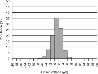 Figure 2. Offset Voltage Production Distribution (G = 128)
 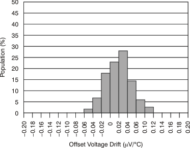 Figure 4. Offset Voltage Drift Distribution (G = 128)
 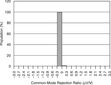 Figure 6. Common-Mode Rejection Distribution (G = 128)
 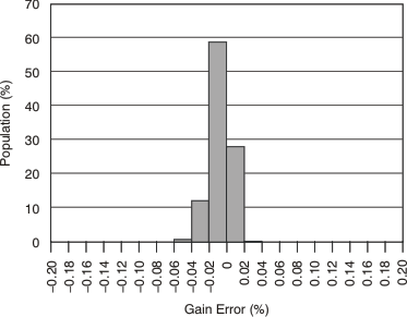 Figure 8. Gain-Error Distribution (G = 128)
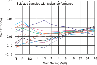
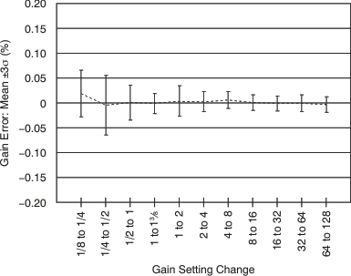 Figure 12. Maximum Gain-Error Deviation Between
Sequential Gain Settings (Mean With ±3 σ)
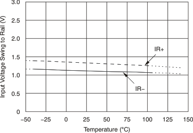
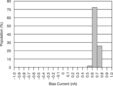 Figure 20. Input Bias Current Distribution (G = 128)
 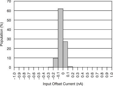 Figure 22. Input Offset Current Distribution (G = 1, G = 128)
 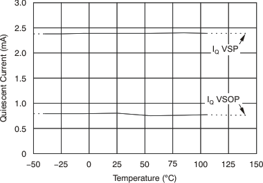 Figure 24. Quiescent Current From Supplies (VSP and VSOP) vs Temperature
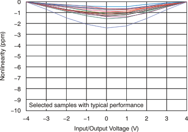
(G = 1)
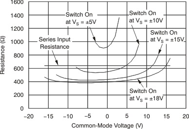 Figure 32. Switch-On Resistance
and Series Input Resistance
vs Common-Mode Voltage at Various Supply Voltages
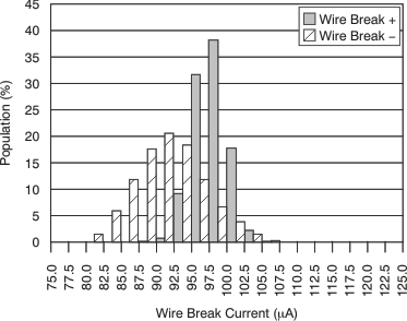 Figure 34. Wire Break Current Distribution
 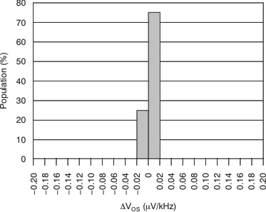 Figure 36. Influence of External Clock Frequency to
VOS Performance (G = 128)
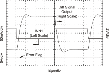
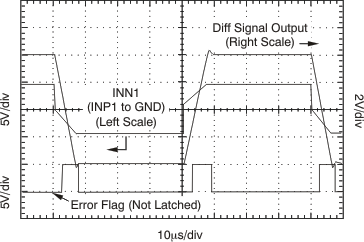
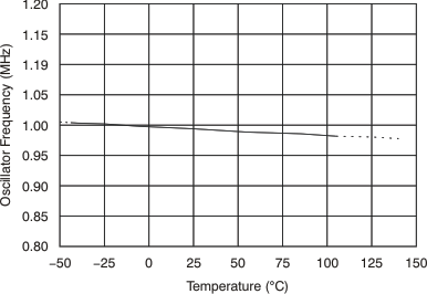
Temperature
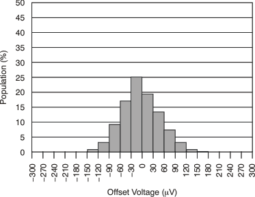 Figure 3. Offset Voltage Production Distribution (G = 1)
 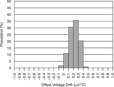 Figure 5. Offset Voltage Drift Distribution (G = 1)
 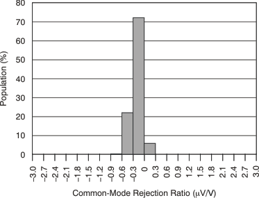 Figure 7. Common-Mode Rejection Distribution (G = 1)
 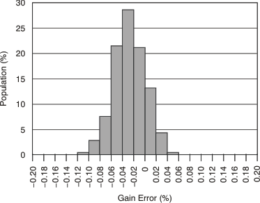 Figure 9. Gain-Error Distribution (G = 1)
 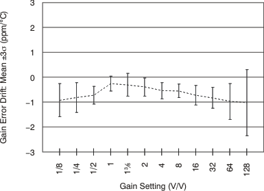 Figure 11. Gain-Error Drift Distribution
vs Gain Setting (Mean With ±3 σ)
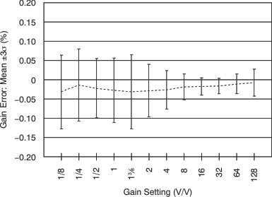
Gain Setting (Mean With ±3σ)
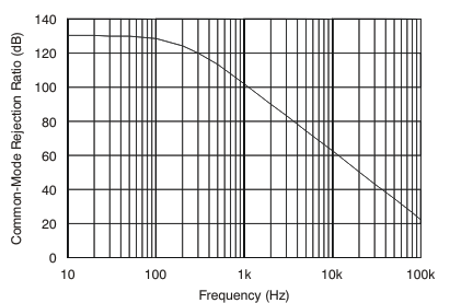
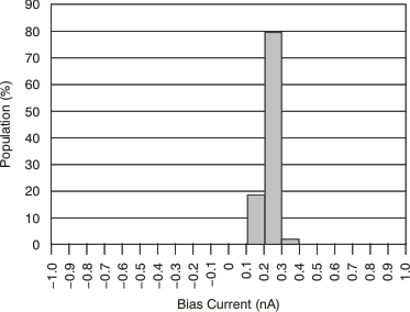 Figure 21. Input Bias Current Distribution (G = 1)
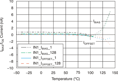
vs Temperature
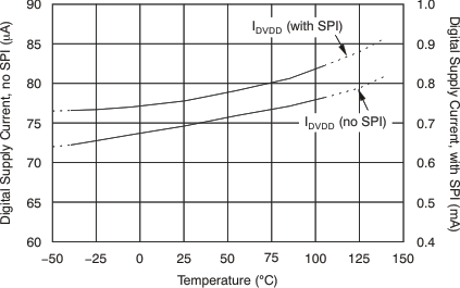 Figure 25. Digital Supply Current
With and Without SPI Communication
vs Temperature
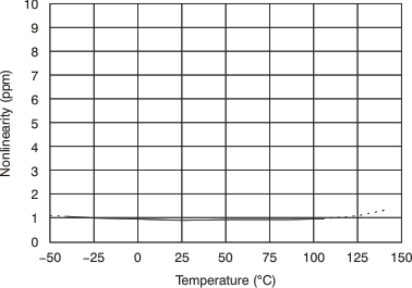
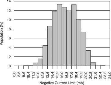
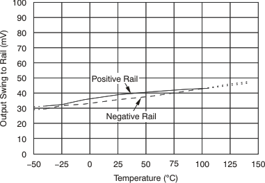
(VSOP – VSON = 5 V)
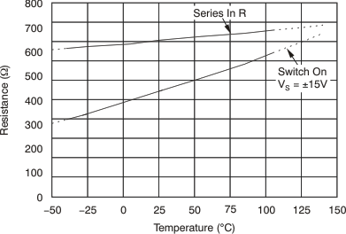 Figure 33. Switch-On Resistance
and Series Input Resistance
vs Temperature
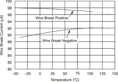
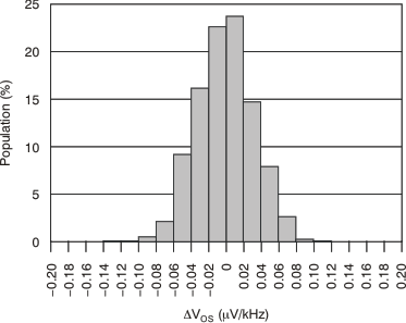 Figure 37. Influence of External Clock Frequency to
VOS Performance (G = 1)
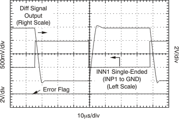
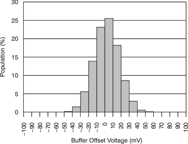 Figure 43. Input Current Buffer Offset Voltage Distribution