SLLS890C August 2008 – April 2024 TL28L92
PRODUCTION DATA
- 1
- 1Features
- 2Description
- 3Pin Configurations and Functions
- 4Electrical Specifications
- 5Detailed Description
-
6Programming
- 6.1 Register Overview
- 6.2 Condensed Register Bit Formats
- 6.3
Register Descriptions
- 6.3.1 Mode Registers
- 6.3.2 Clock Select Registers
- 6.3.3 Command Registers
- 6.3.4 Status Registers
- 6.3.5 Output Configuration Control Register (OPCR)
- 6.3.6 Set Output Port Bits Register (SOPR)
- 6.3.7 Reset Output Port Bits Register (ROPR)
- 6.3.8 Output Port Register (OPR)
- 6.3.9 Auxiliary Control Register (ACR)
- 6.3.10 Input Port Change Register (IPCR)
- 6.3.11 Interrupt Status Register (ISR)
- 6.3.12 Interrupt Mask Register (IMR)
- 6.3.13 Interrupt Vector Register (IVR; 68xxx Mode) or General Purpose Register (GP; 80xxx Mode)
- 6.3.14 Counter and Timer Registers
- 6.4 Output Port Notes
- 6.5 CTS, RTS, CTS Enable Tx Signals
- 7Device and Documentation Support
- 8Revision History
- 9Mechanical, Packaging, and Orderable Information
Package Options
Mechanical Data (Package|Pins)
- FR|44
Thermal pad, mechanical data (Package|Pins)
Orderable Information
2 Description
The TL28L92 operates at 3.3V or 5V supply with added features and deeper FIFOs. The configuration on power-up is 16 character receiver, 16 character transmit FIFOs, watchdog timer for each receiver, mode register 0 is added, extended baud rate and overall faster speeds, programmable receiver and transmitter interrupts.
Pin programming allows the device to operate with either the Motorola or Intel bus interface. The bit 3 of the MR0A register allows the device to operate in an 8 byte FIFO mode.
The Texas Instruments TL28L92 Dual Universal Asynchronous Receiver/Transmitter (DUART) is a single-chip CMOS-LSI communications device that provides two full-duplex asynchronous receiver/transmitter channels in a single package. the device interfaces directly with microprocessors, and can be used in a polled or interrupt driven system with modem and DMA interface.
The operating mode and data format of each channel can be programmed independently. Additionally, each receiver and transmitter can select an operating speed as one of 28 fixed baud rates; a 16× clock derived from a programmable counter/timer, or an external 1× or 16× clock. The baud rate generator and counter/timer can operate directly from a crystal or from external clock inputs. The ability to independently program the operating speed of the receiver and transmitter make the DUART particularly attractive for dual-speed channel applications such as clustered terminal systems.
Each receiver and transmitter is buffered by 8 or 16 character FIFOs to minimize the potential of receiver overrun, transmitter underrun, and to reduce interrupt overhead in interrupt driven systems. In addition, a flow control capability is provided via RTS/CTS signaling to disable a remote transmitter when the receiver buffer is full. Also provided on the TL28L92 is a multipurpose 7-bit input port and a multipurpose 8-bit output port. These can be used as general purpose I/O ports or can be assigned specific functions (such as clock inputs or status/interrupt outputs) under program control.
The TL28L92 is available now in 44-pin QFP (FR).
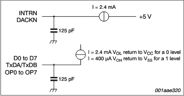
 Test
Conditions on Outputs