JAJSER5B February 2018 – February 2025 LMK05028
PRODUCTION DATA
- 1
- 1 特長
- 2 アプリケーション
- 3 概要
- 4 Pin Configuration and Functions
- 5 Specifications
- 6 Parameter Measurement Information
-
7 Detailed Description
- 7.1 Overview
- 7.2 Functional Block Diagrams
- 7.3
Feature Description
- 7.3.1 Oscillator Input (XO_P/N)
- 7.3.2 TCXO/OCXO Input (TCXO_IN)
- 7.3.3 Reference Inputs (INx_P/N)
- 7.3.4 Clock Input Interfacing and Termination
- 7.3.5 Reference Input Mux Selection
- 7.3.6 Hitless Switching
- 7.3.7 Gapped Clock Support on Reference Inputs
- 7.3.8 Input Clock and PLL Monitoring, Status, and Interrupts
- 7.3.9
PLL Channels
- 7.3.9.1 PLL Frequency Relationships
- 7.3.9.2 Analog PLL (APLL)
- 7.3.9.3 APLL XO Doubler
- 7.3.9.4 APLL Phase Frequency Detector (PFD) and Charge Pump
- 7.3.9.5 APLL Loop Filter
- 7.3.9.6 APLL Voltage Controlled Oscillator (VCO)
- 7.3.9.7 APLL VCO Post-Dividers (P1, P2)
- 7.3.9.8 APLL Fractional N Divider (N) With SDM
- 7.3.9.9 REF-DPLL Reference Divider (R)
- 7.3.9.10 TCXO/OCXO Input Doubler and M Divider
- 7.3.9.11 TCXO Mux
- 7.3.9.12 REF-DPLL and TCXO-DPLL Time-to-Digital Converter (TDC)
- 7.3.9.13 REF-DPLL and TCXO-DPLL Loop Filter
- 7.3.9.14 REF-DPLL and TCXO-DPLL Feedback Dividers
- 7.3.10 Output Clock Distribution
- 7.3.11 Output Channel Muxes
- 7.3.12 Output Dividers
- 7.3.13 Clock Outputs (OUTx_P/N)
- 7.3.14 Glitchless Output Clock Start-Up
- 7.3.15 Clock Output Interfacing and Termination
- 7.3.16 Output Synchronization (SYNC)
- 7.3.17 Zero-Delay Mode (ZDM) Configuration
- 7.3.18 PLL Cascading With Internal VCO Loopback
- 7.4 Device Functional Modes
- 7.5 Programming
- 7.6 Register Maps
- 8 Application and Implementation
- 9 Device and Documentation Support
- 10Revision History
- 11Mechanical, Packaging, and Orderable Information
5.7 Typical Characteristics
Unless otherwise noted: VDD = 3.3 V, VDDO =
1.8 V, TA = 25°C, BWAPLL = 500 kHz, AC-LVPECL output.
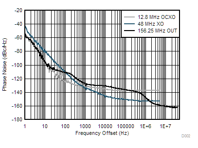
The PLL output clock phase noise at
different frequency offsets are determined by different noise contributors, such
as external clock input sources (REF IN, OCXO, XO) and internal noise sources
(PLL, VCO), as well as the configured PLL loop bandwidths
(BWREF-DPLL, BWTCXO-DPLL, BWAPLL). The phase
noise profile shown for each external clock source (fSOURCE) is
normalized to the PLL output frequency (fOUT) by adding
20×LOG10(fOUT / fSOURCE) to the measured
source's phase noise.


