SLUSFN0A April   2025  – December 2025 BQ25630

PRODUCTION DATA  

  1.   1
  2. Features
  3. Applications
  4. Description
  5. Description (continued)
  6. Device Comparison
  7. Pin Configuration and Functions
  8. Specifications
    1. 7.1 Absolute Maximum Ratings
    2. 7.2 ESD Ratings
    3. 7.3 Recommended Operating Conditions
    4. 7.4 Thermal Information
    5. 7.5 Electrical Characteristics
    6. 7.6 Timing Requirements
    7. 7.7 Typical Characteristics
  9. Detailed Description
    1. 8.1 Overview
    2. 8.2 Functional Block Diagram
    3. 8.3 Feature Description
      1. 8.3.1  Power-On-Reset (POR)
      2. 8.3.2  Device Power Up from Battery
      3. 8.3.3  USB-C Detection
        1. 8.3.3.1 Legacy Adapter Detection
        2. 8.3.3.2 USB-C Dead Battery Mode
        3. 8.3.3.3 SNK Mode
        4. 8.3.3.4 SRC Mode
        5. 8.3.3.5 DRP Mode - Dual Role Port
        6. 8.3.3.6 USB-C Debug Accessory Detection
      4. 8.3.4  Device Power Up from Input Source
        1. 8.3.4.1 REGN LDO Power Up
        2. 8.3.4.2 D+/D– Detection Sets Input Current Limit
        3. 8.3.4.3 Input Voltage Limit Threshold Setting (VINDPM Threshold)
        4. 8.3.4.4 Converter Power-Up
        5. 8.3.4.5 Input Current Optimizer (ICO)
        6. 8.3.4.6 Switching Frequency and Dithering Feature
      5. 8.3.5  Power Path Management
        1. 8.3.5.1 Narrow VDC Architecture
        2. 8.3.5.2 Dynamic Power Management
        3. 8.3.5.3 High Impedance (HIZ) Mode
      6. 8.3.6  Battery Charging Management
        1. 8.3.6.1 Autonomous Charging Cycle
        2. 8.3.6.2 Battery Charging Profile
        3. 8.3.6.3 Charging Termination
        4. 8.3.6.4 Thermistor Qualification
          1. 8.3.6.4.1 Advanced Temperature Profile in Charge Mode
          2. 8.3.6.4.2 TS Pin Thermistor Configuration
          3. 8.3.6.4.3 Cold/Hot Temperature Window in OTG Mode
          4. 8.3.6.4.4 JEITA Charge Rate Scaling
        5. 8.3.6.5 Charging Safety Timers
        6. 8.3.6.6 Alternate Power from Input
      7. 8.3.7  USB On-The-Go (OTG)
        1. 8.3.7.1 Boost OTG Mode
      8. 8.3.8  Integrated 12-bit ADC for Monitoring
      9. 8.3.9  Status Outputs (INT , PG )
        1. 8.3.9.1 PG Pin Power Good Indicator
        2. 8.3.9.2 Interrupts and Status, Flag, and Mask Bits
        3. 8.3.9.3 Interrupt to Host (INT)
      10. 8.3.10 BATFET Control
        1. 8.3.10.1 Shutdown Mode
        2. 8.3.10.2 Ship Mode
        3. 8.3.10.3 Standby Mode
        4. 8.3.10.4 System Power Reset
      11. 8.3.11 Protections
        1. 8.3.11.1 Voltage and Current Monitoring in Battery Only and HIZ Modes
          1. 8.3.11.1.1 Battery Overcurrent Protection
          2. 8.3.11.1.2 Battery Undervoltage Lockout
        2. 8.3.11.2 Voltage and Current Monitoring in Buck Mode
          1. 8.3.11.2.1 Input Overvoltage
          2. 8.3.11.2.2 System Overvoltage Protection (SYSOVP)
          3. 8.3.11.2.3 Forward Converter Cycle-by-Cycle Current Limit
          4. 8.3.11.2.4 System Short
          5. 8.3.11.2.5 Battery Overvoltage Protection (BATOVP)
          6. 8.3.11.2.6 Sleep Comparator
        3. 8.3.11.3 Voltage and Current Monitoring in Boost Mode
          1. 8.3.11.3.1 Boost Mode Overvoltage Protection
          2. 8.3.11.3.2 Boost Mode Duty Cycle Protection
          3. 8.3.11.3.3 Boost Mode PMID Undervoltage Protection
          4. 8.3.11.3.4 Boost Mode Battery Undervoltage
          5. 8.3.11.3.5 Boost Converter Cycle-by-Cycle Current Limit
          6. 8.3.11.3.6 Boost Mode SYS Short
        4. 8.3.11.4 Thermal Regulation and Thermal Shutdown
          1. 8.3.11.4.1 Thermal Protection in Buck Mode
          2. 8.3.11.4.2 Thermal Protection in Boost Mode
          3. 8.3.11.4.3 Thermal Protection in Battery-only Mode
        5. 8.3.11.5 Liquid Detection and Corrosion Mitigation (Patent Pending)
    4. 8.4 Device Functional Modes
      1. 8.4.1 Host Mode and Default Mode
      2. 8.4.2 Register Bit Reset
    5. 8.5 Programming
      1. 8.5.1 Serial Interface
        1. 8.5.1.1 Data Validity
        2. 8.5.1.2 START and STOP Conditions
        3. 8.5.1.3 Byte Format
        4. 8.5.1.4 Acknowledge (ACK) and Not Acknowledge (NACK)
        5. 8.5.1.5 Target Address and Data Direction Bit
        6. 8.5.1.6 Single Write and Read
        7. 8.5.1.7 Multi-Write and Multi-Read
    6. 8.6 Register Maps
      1. 8.6.1 Register Programming
      2. 8.6.2 BQ25630 Registers
  10. Application and Implementation
    1. 9.1 Application Information
    2. 9.2 Typical Application
      1. 9.2.1 Design Requirements
      2. 9.2.2 Detailed Design Procedure
        1. 9.2.2.1 Inductor Selection
        2. 9.2.2.2 Input Capacitor
        3. 9.2.2.3 Output Capacitor
      3. 9.2.3 Application Curves
    3. 9.3 Power Supply Recommendations
    4. 9.4 Layout
      1. 9.4.1 Layout Guidelines
      2. 9.4.2 Layout Example
  11. 10Device and Documentation Support
    1. 10.1 Device Support
      1. 10.1.1 Third-Party Products Disclaimer
    2. 10.2 Documentation Support
      1. 10.2.1 Related Documentation
    3. 10.3 Receiving Notification of Documentation Updates
    4. 10.4 Support Resources
    5. 10.5 Trademarks
    6. 10.6 Electrostatic Discharge Caution
    7. 10.7 Glossary
  12. 11Revision History
  13. 12Mechanical, Packaging, and Orderable Information

Host Mode and Default Mode

The device is a host controlled charger, but the device can operate in default mode without host management. In default mode, the device can be used as an autonomous charger with no host or while host is in sleep mode. When the charger is in default mode, WD_STAT bit becomes HIGH, WD_FLAG is set to 1b, and an INT is asserted low to alert the host (unless masked by WD_MASK). The WD_FLAG bit reads as 1b upon the first read and then 0b upon subsequent reads. When the charger is in host mode, WD_STAT bit is LOW.

After power-on-reset, the device starts in default mode with watchdog timer expired. All the registers are in the default settings.

In default mode, the device keeps charging the battery with default 1-hour trickle charging safety timer, 2-hour pre-charging safety timer and the 12-hour fast charging safety timer. If any of these timers expire, charging is stopped and the buck converter continues to operate to supply the system load.

A write to any I2C register transitions the charger from default mode to host mode, and initiates the watchdog timer. All the device parameters can be programmed by the host. To keep the device in host mode, the host has to reset the watchdog timer by writing 1b to WD_RST bit before the watchdog timer expires (WD_STAT bit is set), or disable watchdog timer by setting WATCHDOG bits = 00b.

When the watchdog expires, the device returns to default mode. The ICHG value is divided in half when the watchdog timer expires, and a number of other fields are reset to the POR default values as shown in the notes column of the register tables in Section 8.6.2. The watchdog timer is reset on any write if the watchdog timer has expired. When watchdog timer expires, WD_STAT and WD_FLAG are set to 1b, and an INT is asserted low to alert the host (unless masked by WD_MASK). If WD_MODE bit is set to 1b and the watchdog timer expires, a system reset occurs.
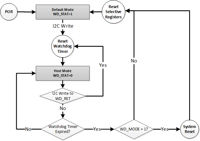
Figure 8-10 Watchdog Timer Flow Chart BQ25630