SPRACS0A May 2020 – November 2022 TMS320F280048-Q1 , TMS320F280048C-Q1 , TMS320F280049 , TMS320F280049-Q1 , TMS320F280049C , TMS320F280049C-Q1 , TMS320F28033 , TMS320F28033-Q1 , TMS320F28035 , TMS320F28035-EP , TMS320F28035-Q1 , TMS320F28053 , TMS320F28055 , TMS320F2806-Q1 , TMS320F28065 , TMS320F28069 , TMS320F28069-Q1 , TMS320F28069F , TMS320F28069F-Q1 , TMS320F28069M , TMS320F28069M-Q1 , TMS320F28075 , TMS320F28075-Q1 , TMS320F28076 , TMS320F28374D , TMS320F28374S , TMS320F28375D , TMS320F28375S , TMS320F28375S-Q1 , TMS320F28376D , TMS320F28376S , TMS320F28377D , TMS320F28377D-EP , TMS320F28377D-Q1 , TMS320F28377S , TMS320F28377S-Q1 , TMS320F28378D , TMS320F28378S , TMS320F28379D , TMS320F28379D-Q1 , TMS320F28379S , TMS320F28384D , TMS320F28384D-Q1 , TMS320F28384S , TMS320F28384S-Q1 , TMS320F28386D , TMS320F28386D-Q1 , TMS320F28386S , TMS320F28386S-Q1 , TMS320F28388D , TMS320F28388S , TMS320F28P650DH , TMS320F28P650DK , TMS320F28P650SH , TMS320F28P650SK , TMS320F28P659DH-Q1 , TMS320F28P659DK-Q1 , TMS320F28P659SH-Q1
3 Low interrupt Latency of CLA
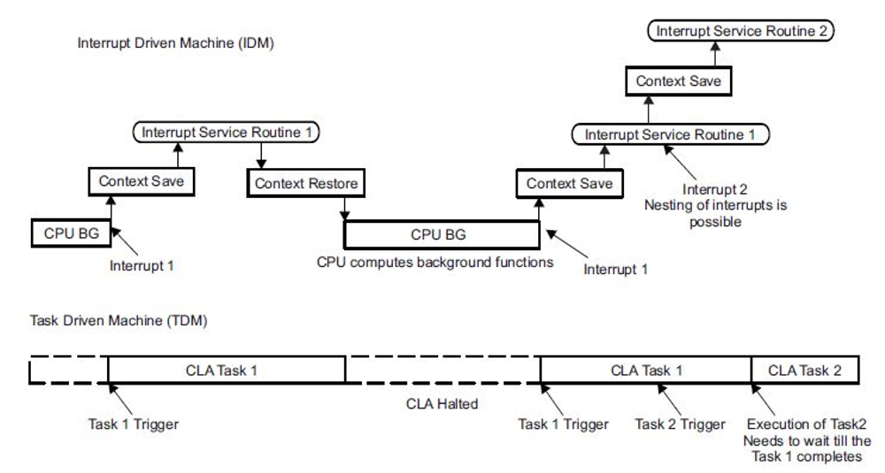
In any real-time control application, the sample to output delay, defined as the time that elapses between sensing, processing and actuation, is an important system consideration. The low-latency architecture of CLA reduces this sample to output time while increasing the overall system throughput. This is made possible because CLA is task oriented instead of interrupt driven machine and does not use interrupts to synchronize with hardware. Instead, it supports up to eight independent tasks, which are each mapped to hardware events such as a timer or data availability on an ADC, and so forth. A task initiated on the CLA runs to completion without any interruption or nesting involved, hence eliminating the need for any context-switching overhead typically involved in traditional interrupt-based processors. Thus, there is little to no delay involved in processing the data by CLA, which ultimately reduces the sample to output delay and enables faster system response. Figure 3-1 illustrates the differences between a task driven machine (TDM) and an interrupt driven machine (IDM).
 Figure 3-1 Interrupt vs Task Driven
Machine
Figure 3-1 Interrupt vs Task Driven
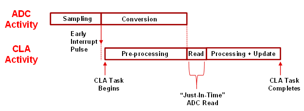
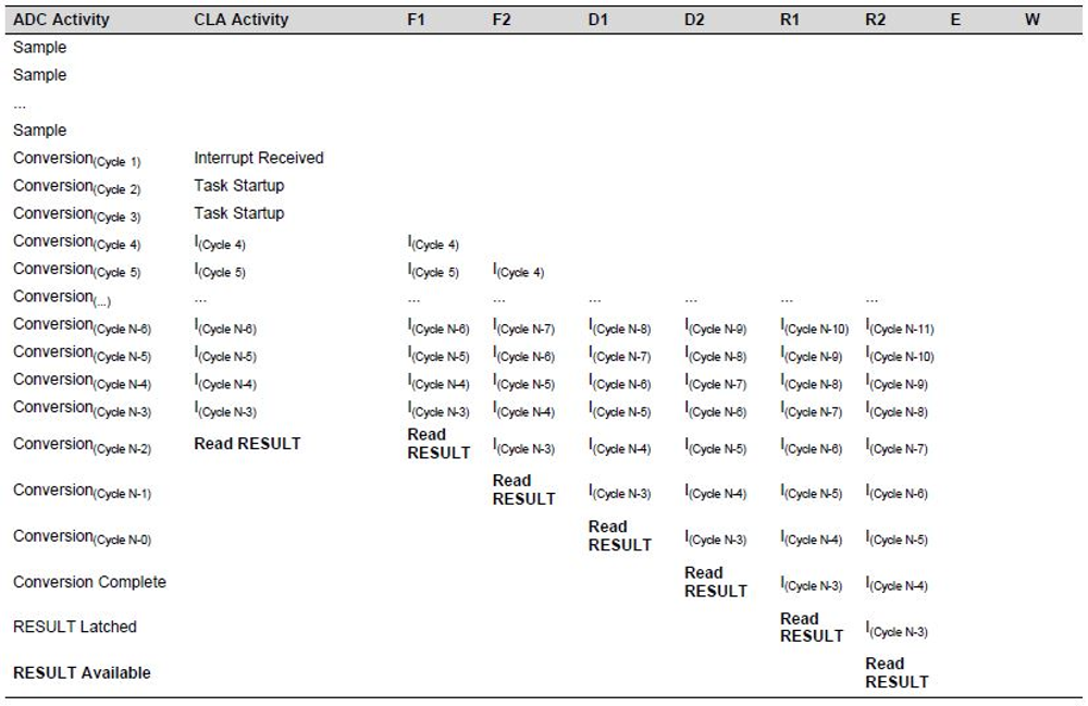
MachineThe low interrupt response of CLA can be leveraged in combination with the early-interrupt feature of TI’s internal ADC to further reduce the sample to output delay. The ADC can be configured to generate an early interrupt pulse at the end of sampling before the conversion completes. This early-interrupt pulse from the ADC can be used to trigger a CLA task that would allow the CLA to read the result as soon as the conversion result is available in the ADC result register. This combination of just-in-time sampling along with the low interrupt response of the CLA enable faster system response and higher frequency control loops. The available time before the conversion can be effectively utilized for any necessary pre-processing steps within the CLA task as illustrated in Figure 3-2. The exact instruction at which the read request should be placed to achieve just-in-time read can be calculated based on the CLA pipeline activity for N-cycle ADC conversion. As shown in Figure 3-3, The N-2 instruction will arrive in the R2 phase just in time to read the result register. For the standard 12-bit ADC configuration and clock divider as 4, N is 42. To find out the correct value of N based on the configuration of ADC, see the device-specific data sheet [4].
 Figure 3-2 Early Interrupt From ADC to
Trigger CLA Task
 Figure 3-3 CLA Pipeline Activity for
Early Interrupt Pulse
Figure 3-3 CLA Pipeline Activity for
Early Interrupt PulseThe example “cla_ex5_adc_just_in_time” utilizes the above concept to read the ADC data “just-in-time” even at very high sampling frequencies. As depicted in Figure 3-4, EPWM1 is configured to generate a PWM output signal of frequency 1 MHz, which is also used to trigger the ADC sampling at each cycle. The example also utilizes the newly added feature in TI’s Type 5 ADCs, which allows delaying the early interrupt pulse by few cycles as per the programmed OFFSET value. Thus ADCA is configured to sample the input on Channel 0 and to generate the early interrupt at the end of S/H + offset cycles. This interrupt is used to trigger the CLA control task. The CLA task implements the control logic to update the duty of the PWM output based on the read ADC value. The early interrupt feature and low interrupt latency of CLA allows the application to do any necessary pre-work so that the application can act on the ADC results immediately when they become available and still complete updating the PWM output before the next interrupts arrives. Thus, all the three steps (sampling, processing and actuation) are completed within a 1 MHz cycle. As shown in the below code snippet of the CLA task, 3-point moving average filter is used to simulate the processing sequence for illustration purposes and few steps of the filtering sequence that are denoted as the pre-processing code are implemented before reading the ADC result to make use of the time available before conversion.
 Figure 3-4 “Just-in-time” ADC Read
Example Showcase
 //
// Pre-processing for implementing moving average filter, takes 13 cycles
// This is just to illustrate how cycles can be utilized to do some pre-
// processing before ADC result latches. Based on the cycles taken by
// pre-processing code, ADC interrupt offset need to be programmed
//
data_read_total = data_read + data_read_prev;
data_read_prev2 = data_read_prev;
data_read_prev = data_read;
//
// Reading ADC just-in-time
//
data_read = HWREGH(ADCARESULT_BASE + ADC_RESULTx_OFFSET_BASE + ADC_SOC_NUMBER0);
//
// "data_read_total" stores the cumulative sum of current and last 2 data elements
//
data_read_total += data_read;
//
// Taking average of 3 elements, normalizing for 12-bit and mapping to output duty
// linearly in the range 0.1-0.9
// duty = 0.1 + (0.9-0.1) * ((data_read_total / 3) / 2^12 )
//
duty = 0.1f + (data_read_total / (15360.0f));
//
// Writing to the COMPA register for realizing computed duty value
//
HWREGH(EPWM1_BASE + EPWM_O_CMPA + 0x1U) = (uint16_t)(duty * EPWM1_PERIOD + 0.5f);The early interrupt OFFSET value of ADC need to be adjusted based on the cycles consumed by the pre-processing in order to read the ADC data “just-in-time”. In this example, the OFFSET value of 20 is used based on the calculation shown in example header. The programming sequence for this configuration of ADC is shown below. The actual use-case may involve different pre-processing steps, hence the interrupt OFFSET value need to programmed accordingly.
    //
    // Set pulse positions to early
    //
    ADC_setInterruptPulseMode(ADCA_BASE, ADC_PULSE_END_OF_ACQ_WIN);
    //
    // Set interrupt offset delay as 20 cycles based on the calculation
    // shown in example header
    //
    ADC_setInterruptCycleOffset(ADCA_BASE, 20);