SBOU024C august 2004 – july 2023 PGA309
- 1
- Read This First
-
1Introduction
- 1.1 PGA309 Functional Description
- 1.2 Sensor Error Adjustment Range
- 1.3 Gain Scaling
- 1.4 Offset Adjustment
- 1.5 Voltage Reference
- 1.6 Sensor Excitation and Linearization
- 1.7 ADC for Temperature Sensing
- 1.8 External EEPROM and Temperature Coefficients
- 1.9 Fault Monitor
- 1.10 Over-Scale and Under-Scale Limits
- 1.11 Power-Up and Normal Operation
- 1.12 Digital Interface
- 1.13 Pin Configuration
- 2Detailed Description
- 3Operating Modes
-
4Digital Interface
- 4.1 Description
- 4.2 Two-Wire Interface
- 4.3 One-Wire Interface
- 4.4 One-Wire Interface Timeout
- 4.5 One-Wire Interface Timing Considerations
- 4.6 Two-Wire Access to External EEPROM
- 4.7 One-Wire Interface Initiated Two-Wire EEPROM Transactions
- 4.8 PGA309 Stand-Alone Mode and Two-Wire Transactions
- 4.9 PGA309 Two-Wire Bus Master Operation and Bus Sharing Considerations
- 4.10 One-Wire Operation with PRG Connected to VOUT
- 4.11 Four-Wire Modules and One-Wire Interface (PRG)
- 5Application Background
-
6Register Descriptions
- 6.1 Internal Register Overview
- 6.2
Internal Register Map
- 6.2.1 Register 0: Temp ADC Output Register (Read Only, Address Pointer = 00000)
- 6.2.2 Register 1: Fine Offset Adjust (Zero DAC) Register (Read/Write, Address Pointer = 00001)
- 6.2.3 Register 2: Fine Gain Adjust (Gain DAC) Register (Read/Write, Address Pointer = 00010)
- 6.2.4 Register 3: Reference Control and Linearization Register (Read/Write, Address Pointer = 00011)
- 6.2.5 Register 4: PGA Coarse Offset Adjust and Gain Select/Output Amplifier Gain Select Register (Read/Write, Address Pointer = 00100)
- 6.2.6 Register 5: PGA Configuration and Over/Under-Scale Limit Register (Read/Write, Address Pointer = 00101)
- 6.2.7 Register 6: Temp ADC Control Register (Read/Write, Address Pointer = 00110)
- 6.2.8 Register 7: Output Enable Counter Control Register (Read/Write, Address Pointer = 00111)
- 6.2.9 Register 8: Alarm Status Register (Read Only, Address Pointer = 01000)
- A External EEPROM Example
- B Detailed Block Diagram
- C Glossary
- Revision History
2.7 Temperature Measurement
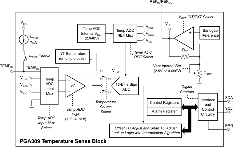
The center of the PGA309 temperature measurement circuitry is the Temp ADC. The Temp ADC and its associated PGA, input mux, and REF mux provide a flexible and configurable temperature sensing block for reading either on-chip or external temperatures. Figure 2-15 illustrates the PGA309 temperature sense block.
The internal temperature sensing is accomplished by using on-chip diode junctions. The Internal Temperature Mode is configured through setting the bits in Register 6 to the values shown in Table 2-7 and Table 2-8. The Temp ADC output is presented in Register 0 in 12-bit + sign extended, right-justified, two’s complement data format (see Table 2-9). The resolution, for the Temp ADC in Internal Temperature Mode, is 0.0625°C/count and the accuracy is ±2°C. The temperature accuracy is a relative error that is calibrated out with the PGA309 + sensor calibration to the accuracy of the calibration temperature measurement equipment.
 Figure 2-15 Temperature Sense Block
| Bit | Bit Name | Bit State | Configuration |
|---|---|---|---|
| 15 | RFB | 0 | Reserved Factory Bit—set to 0 for proper operation |
| 14 | RFB | 0 | Reserved Factory Bit—set to 0 for proper operation |
| 13 | ADC2X | 0 | Unused for Internal Temperature Mode; set to zero. |
| 12 | ADCS | 0 | |
| 11 | ISEN | 0 | |
| 10 | CEN | 1 | Enable the Temp ADC |
| 9 | TEN | 1 | Internal Temperature Mode selected |
| 8 | AREN | 0 | Unused for Internal Temperature Mode; set to zero. |
| 7 | RV1 | 0 | |
| 6 | RV0 | 0 | |
| 5 | M1 | 0 | |
| 4 | M0 | 0 | |
| 3 | G1 | 0 | |
| 2 | G0 | 0 | |
| 1 | R1 | 1 | See Table 2-8. |
| 0 | R0 | 1 | See Table 2-8. |
| R1 | R0 | Temp ADC Resolution (Conversion Time) Select TEN = ‘1’ |
|---|---|---|
| 0 | 0 | 9-Bit + Sign, Right-Justified, Sign-Extended, Twos Complement, 0.5°C (3ms) |
| 0 | 1 | 10-Bit + Sign, Right-Justified, Twos Complement, Sign-Extended, 0.25°C (6ms) |
| 1 | 0 | 11-Bit + Sign, Right-Justified, Twos Complement, Sign-Extended, 0.125°C (12ms) |
| 1 | 1 | 12-Bit + Sign, Right-Justified, Twos Complement, Sign-Extended, 0.0625°C (24ms) |
| Temperature (°C) | Digital Output (Binary) AD15…………AD0 | Digital Output (Hex) |
|---|---|---|
| 128 | 0000 1000 0000 0000 | 0800 |
| 127.9375 | 0000 0111 1111 1111 | 07FF |
| 100 | 0000 0110 0100 0000 | 0640 |
| 80 | 0000 0101 0000 0000 | 0500 |
| 75 | 0000 0100 1011 0000 | 04B0 |
| 50 | 0000 0011 0010 0000 | 0320 |
| 25 | 0000 0001 1001 0000 | 0190 |
| 0.25 | 0000 0000 0000 0100 | 0004 |
| 0.0 | 0000 0000 0000 0000 | 0000 |
| −0.25 | 1111 1111 1111 1100 | FFFC |
| −25 | 1111 1110 0111 0000 | FE70 |
| −55 | 1111 1100 1001 0000 | FC90 |
| −128 | 1111 1000 0000 0000 | F800 |
For Positive Temperatures (for example, +50°C):
Twos Complement is not performed on positive numbers. Therefore, simply convert the number to binary code with the 16-bit, right-justified format, and MSB = 0 to denote a positive sign. Extend this sign into the upper 4 bits.
Example: (50°C)/(0.0625°C/count) = 800 = 320h = 0011 0010 0000 Twos Complement 16-bit, right-justified, sign-extended format = 0000 0011 0010 0000 = 0320h.
For Negative Temperatures (for example, −25°C):
Generate the Twos Complement of a negative number by complementing the absolute value binary number and adding 1. Extend the sign, denoting a negative number with MSB = 1. Extend the sign to the upper 4 bits to form the 16-bit word.
Example: (| −25°C|)/(0.0625°C/count) = 400 = 190h = 0001 1001 0000 Twos Complement format: 1110 0111 0000 Extend the sign and create the 16-bit word: 1111 1110 0111 0000 = FE70h
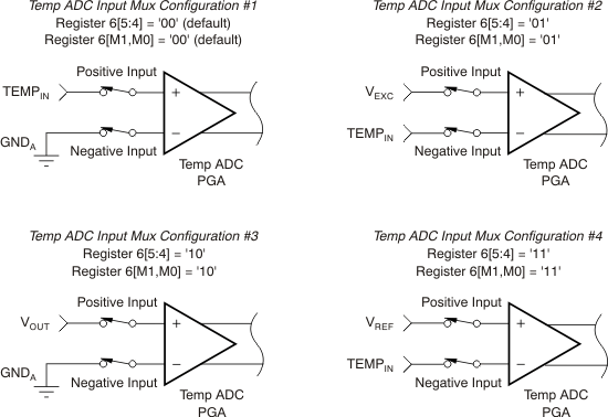
There are several configurations possible for the Temp ADC when External Temperature Mode is selected. In this mode, the TEMPIN pin is read to determine temperature. TEMPIN may be referenced to GND, VEXC, or VREF. VOUT may also be selected to be read relative to GND through the Temp ADC. Figure 2-16 shows the allowable Temp ADC input mux configurations.
In Configuration #3, the VOUT pin is read, not the VFB pin. Therefore, this value may be different from VOUT FILT. Refer to Figure 1-1 and Figure 2-5.
 Figure 2-16 Temp ADC Input Mux Options
| G1 [3] | G0 [2] | Temp ADC PGA Gain |
|---|---|---|
| 0 | 0 | 1 |
| 0 | 1 | 2 |
| 1 | 0 | 4 |
| 1 | 1 | 8 |
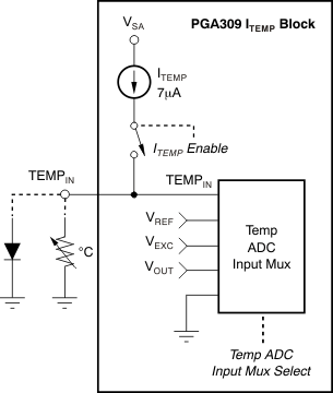
The temperature sense block also contains a 7µA (typ) current source, ITEMP, that is enabled by a logic ‘1’ written to Register 6, bit 11, ISEN. A logic ‘0’ disables ITEMP from the TEMPIN pin. This current source can be used to excite an external resistive temperature device or diode for bridge sensor temperature measurement, as shown in Figure 2-17.
 Figure 2-17 ITEMP for External Temperature Measurement
The Temp ADC has several choices for its reference voltage for analog-to-digital conversions when used in External Temperature mode; these are illustrated in Table 2-11 and Figure 2-15. The resolution of the Temp ADC when used in External Temperature mode is also register-selectable (see Table 2-12).
| AREN [8] | RV1 [7] | RV0 [6] | Temp ADC Reference (VREFT) |
|---|---|---|---|
| 0 | 0 | 0 | VREF |
| 0 | 0 | 1 | VEXC |
| 0 | 1 | 0 | VSA |
| 0 | 1 | 1 | Factory Reserved |
| 1 | X(1) | X(1) | Temp ADC Internal REF (2.048V) |
| R1 [1] | R0 [0] | External Signal Mode [TEN=0], External Reference [AREN=0] | External Signal Mode [TEN=0], Internal Reference [2.048V, AREN=1] |
|---|---|---|---|
| 0 | 0 | 11-Bit + Sign, Right-Justified, Sign-Extended (6ms) | 11-Bit + Sign, Right-Justified, Sign-Extended (8ms) |
| 0 | 1 | 13-Bit + Sign, Right-Justified, Sign-Extended (24ms) | 13-Bit + Sign, Right-Justified, Sign-Extended (32ms) |
| 1 | 0 | 14-Bit + Sign, Right-Justified, Sign-Extended (50ms) | 14-Bit + Sign, Right-Justified, Sign-Extended (64ms) |
| 1 | 1 | 15-Bit + Sign, Right-Justified, Sign-Extended (100ms) | 15-Bit + Sign, Right-Justified, Sign-Extended (128ms) |