SBOU024C august 2004 – july 2023 PGA309
- 1
- Read This First
-
1Introduction
- 1.1 PGA309 Functional Description
- 1.2 Sensor Error Adjustment Range
- 1.3 Gain Scaling
- 1.4 Offset Adjustment
- 1.5 Voltage Reference
- 1.6 Sensor Excitation and Linearization
- 1.7 ADC for Temperature Sensing
- 1.8 External EEPROM and Temperature Coefficients
- 1.9 Fault Monitor
- 1.10 Over-Scale and Under-Scale Limits
- 1.11 Power-Up and Normal Operation
- 1.12 Digital Interface
- 1.13 Pin Configuration
- 2Detailed Description
- 3Operating Modes
-
4Digital Interface
- 4.1 Description
- 4.2 Two-Wire Interface
- 4.3 One-Wire Interface
- 4.4 One-Wire Interface Timeout
- 4.5 One-Wire Interface Timing Considerations
- 4.6 Two-Wire Access to External EEPROM
- 4.7 One-Wire Interface Initiated Two-Wire EEPROM Transactions
- 4.8 PGA309 Stand-Alone Mode and Two-Wire Transactions
- 4.9 PGA309 Two-Wire Bus Master Operation and Bus Sharing Considerations
- 4.10 One-Wire Operation with PRG Connected to VOUT
- 4.11 Four-Wire Modules and One-Wire Interface (PRG)
- 5Application Background
-
6Register Descriptions
- 6.1 Internal Register Overview
- 6.2
Internal Register Map
- 6.2.1 Register 0: Temp ADC Output Register (Read Only, Address Pointer = 00000)
- 6.2.2 Register 1: Fine Offset Adjust (Zero DAC) Register (Read/Write, Address Pointer = 00001)
- 6.2.3 Register 2: Fine Gain Adjust (Gain DAC) Register (Read/Write, Address Pointer = 00010)
- 6.2.4 Register 3: Reference Control and Linearization Register (Read/Write, Address Pointer = 00011)
- 6.2.5 Register 4: PGA Coarse Offset Adjust and Gain Select/Output Amplifier Gain Select Register (Read/Write, Address Pointer = 00100)
- 6.2.6 Register 5: PGA Configuration and Over/Under-Scale Limit Register (Read/Write, Address Pointer = 00101)
- 6.2.7 Register 6: Temp ADC Control Register (Read/Write, Address Pointer = 00110)
- 6.2.8 Register 7: Output Enable Counter Control Register (Read/Write, Address Pointer = 00111)
- 6.2.9 Register 8: Alarm Status Register (Read Only, Address Pointer = 01000)
- A External EEPROM Example
- B Detailed Block Diagram
- C Glossary
- Revision History
2.4 Output Amplifier
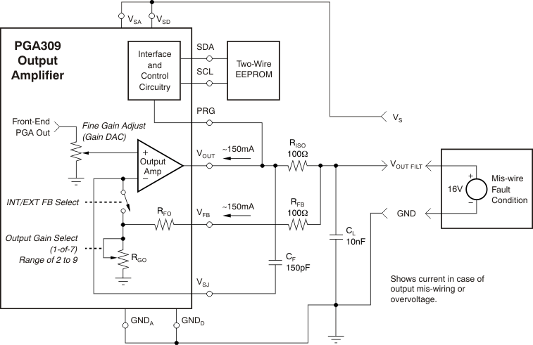
The Output Amplifier section of the PGA309 is configured to allow maximum flexibility and accuracy in the end application. Figure 2-5 depicts the Output Amplifier in a common three-terminal sensor application. In this application, it is desired to provide overvoltage protection due to mis-wires on the output of the PGA309, as well as a 10nF capacitor on the sensor module output for EMI/RFI filtering. In this configuration, RISO and RFB provide overvoltage protection on VOUT FILT to 16V by limiting the current into VOUT and VFB to about 150mA [(16V − 0.7V)/100Ω]. The 0.7V drop results from the internal ESD structure to GND or VSA. In addition, RISO serves to isolate the 10nF RFI/ EMI capacitive load from VOUT. RFB adds a slight gain error that is calibrated out with the PGA309 + sensor calibration. Note that the point of feedback around the Output Amplifier is taken from VOUT FILT and as such, after PGA309 + sensor calibration, the Output Amplifier will accurately scale VOUTFILT to match the desired conditioned sensor voltage. CF provides a second feedback path around the Output Amplifier for stability. With the configuration shown, the Output Amplifier is stable for internal Output Amplifier gains from 2 (125kHz bandwidth, 63° loop gain phase margin, typical values) to 9 (64kHz bandwidth, 86° loop gain phase margin, typical values). Table 2-1 details the typical Output Amplifier resistor values for RFO and RGO, as well as open-loop output resistance. These values, combined with the typical Output Amplifier open-loop gain curve and standard op amp stability techniques, allow the Output Amplifier to be tailored and configured for the specific sensor application.
 Figure 2-5 Output Amplifier in a Common 3-Terminal Sensor Application
| Gain | RFO
Typical (kΩ) |
RGO
Typical (kΩ) |
|---|---|---|
| 2 | 18 | 18 |
| 2.4 | 21 | 15 |
| 3 | 24 | 12 |
| 3.6 | 26 | 10 |
| 4.5 | 28 | 8 |
| 6 | 30 | 6 |
| 9 | 32 | 4 |
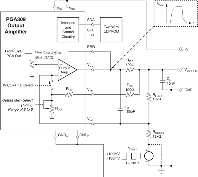
In addition to using its own internal gain setting resistors, RFO and RGO, the Output Amplifier may use external feedback resistors RFOEXT and RGOEXT, as shown in Figure 2-6. Table 2-2 details the bits used in Register 4 for the desired Output Amplifier gain configurations. To use the external feedback resistors, set GO2, GO1, and GO0 to all 1s. In addition to allowing external feedback resistors to be used, this configuration provides a handy mechanism for testing the Output Amplifier stability, even if internal gain settings are to be used. As shown in Figure 2-6, external feedback resistors RFOEXT and RGOEXT are both set to 18kΩ, equivalent to the typical resistor values used for an internal gain setting of 2. If VOUT is biased to mid-scale (+2.5V for VSA = +5V) through the Zero DAC and by setting VDIFF = 0V, a signal generator may be used to inject a 200mVPP square wave (1kHz) into the end of RGOEXT and a response measured at VOUT. This provides a transient response for the Output Amplifier in a given configuration. Standard stability transient response criteria for a dominant two-pole system may be used to determine suitable phase margin based upon the measured overshoot and ringing on VOUT.
 Figure 2-6 Output Amplifier Using External Feedback Resistors RFOEXT and RGOEXT
| GO2 [14] |
GO1 [13] |
GO0 [12] |
Output Amplifier Gain |
|---|---|---|---|
| 0 | 0 | 0 | 2 |
| 0 | 0 | 1 | 2.4 |
| 0 | 1 | 0 | 3 |
| 0 | 1 | 1 | 3.6 |
| 1 | 0 | 0 | 4.5 |
| 1 | 0 | 1 | 6 |
| 1 | 1 | 0 | 9 |
| 1 | 1 | 1 | Disable Internal Feedback |
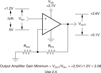
For low-supply applications, the minimum gain for the Output Amplifier is related to its IVR and output voltage swing. In Figure 2-7, the supply is lowered to +2.7V. The tested IVR of the Output Amplifier is 0V to VSA−1.5V, as reflected in Figure 2-7. The output voltage swing is tested to be 0.1V to +2.6V for a 10kΩ load, as shown. This calculates to a minimum gain of 2.08. For best performance, the Output Amplifier should be scaled for a minimum gain of 2.4 for this application. Usually, this is only a factor at lower voltages but is easily checked for each individual application.
 Figure 2-7 Output Amplifier Minimum Gain at Low Supply