SBOU024C august 2004 – july 2023 PGA309
- 1
- Read This First
-
1Introduction
- 1.1 PGA309 Functional Description
- 1.2 Sensor Error Adjustment Range
- 1.3 Gain Scaling
- 1.4 Offset Adjustment
- 1.5 Voltage Reference
- 1.6 Sensor Excitation and Linearization
- 1.7 ADC for Temperature Sensing
- 1.8 External EEPROM and Temperature Coefficients
- 1.9 Fault Monitor
- 1.10 Over-Scale and Under-Scale Limits
- 1.11 Power-Up and Normal Operation
- 1.12 Digital Interface
- 1.13 Pin Configuration
- 2Detailed Description
- 3Operating Modes
-
4Digital Interface
- 4.1 Description
- 4.2 Two-Wire Interface
- 4.3 One-Wire Interface
- 4.4 One-Wire Interface Timeout
- 4.5 One-Wire Interface Timing Considerations
- 4.6 Two-Wire Access to External EEPROM
- 4.7 One-Wire Interface Initiated Two-Wire EEPROM Transactions
- 4.8 PGA309 Stand-Alone Mode and Two-Wire Transactions
- 4.9 PGA309 Two-Wire Bus Master Operation and Bus Sharing Considerations
- 4.10 One-Wire Operation with PRG Connected to VOUT
- 4.11 Four-Wire Modules and One-Wire Interface (PRG)
- 5Application Background
-
6Register Descriptions
- 6.1 Internal Register Overview
- 6.2
Internal Register Map
- 6.2.1 Register 0: Temp ADC Output Register (Read Only, Address Pointer = 00000)
- 6.2.2 Register 1: Fine Offset Adjust (Zero DAC) Register (Read/Write, Address Pointer = 00001)
- 6.2.3 Register 2: Fine Gain Adjust (Gain DAC) Register (Read/Write, Address Pointer = 00010)
- 6.2.4 Register 3: Reference Control and Linearization Register (Read/Write, Address Pointer = 00011)
- 6.2.5 Register 4: PGA Coarse Offset Adjust and Gain Select/Output Amplifier Gain Select Register (Read/Write, Address Pointer = 00100)
- 6.2.6 Register 5: PGA Configuration and Over/Under-Scale Limit Register (Read/Write, Address Pointer = 00101)
- 6.2.7 Register 6: Temp ADC Control Register (Read/Write, Address Pointer = 00110)
- 6.2.8 Register 7: Output Enable Counter Control Register (Read/Write, Address Pointer = 00111)
- 6.2.9 Register 8: Alarm Status Register (Read Only, Address Pointer = 01000)
- A External EEPROM Example
- B Detailed Block Diagram
- C Glossary
- Revision History
 Figure 2-14 Corrected Bridge Parabolic Nonlinearity vs Pressure
In each end application, the Linearization Circuit limits should be checked for operation within the allowed range.
Table 2-5 and Table 2-6 illustrate the linearization range for several typical system applications. These tables account for the internal limits of the PGA309 linearization circuit and assume that VOUT scaling is to account for over-scale and under-scale limits and fault detection. For specific end applications not listed, the following equations may be used to calculate critical design values, once the system design choices for VREF, VOUTMAX,VOUTMIN and linearization range, are made:
- VEXC MAX: Use Equation 7 at VOUT MAX
- VEXC MIN: Use Equation 7 at VOUT MIN
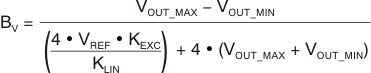
- BVMAX (maximum nonlinearity that can be compensated): Use KLIN+MAX to calculate +BVMAX and KLIN–MAX to calculate –BVMAX by Equation 4 solved for BV as:
- For Range 0:
KLIN −MAX = −0.166
KLIN +MAX = +0.166 - For Range 1:
KLIN −MAX = −0.124
KLIN +MAX = +0.124
- For Range 0:
- VLin DAC MAX = ((VREF/4) – VOUT MAX/10) ≥ 300mV
- VEXC MAX ≤ VSA − 0.5V
- KLIN −MAX ≤ KLIN ≤ KLIN +MAX
When using the Linearization Circuit, to ensure that the bridge sensor output common-mode voltage remains within the PGA309 input specifications, Equation 7 can be used to calculate VEXC at full-scale signal (VOUT MAX). The common-mode voltage (VCM) of the bridge sensor output is one-half of VEXC if no common-mode or temperature sensing additional resistor is used in series with the bridge sensor.
During the sensor calibration process using the PGA309, a two-step process can be employed. First, the nonlinearity of the sensor bridge is measured with an initial gain and offset and with KLIN = 0 (Lin DAC set to Zero). Using the resulting sensor nonlinearity (BV), values for KLIN, Gain, and Offset are calculated. A second calibration measurement can be taken to adjust KLIN, to account for any offsets and mismatches in the Linearization Circuit. This calibration procedure is most easily performed using the PGA309 Designer’s Kit and associated software and calibration spreadsheets, which can be downloaded from www.ti.com.
| Case1 | Case2 | Case3 | Case4 | |
|---|---|---|---|---|
| 0.057 | 0.075 | 0.112 | 0.075 | KLIN +MAX |
| Range 0 | |||||
|---|---|---|---|---|---|
| KEXC | 0.83 | FSS | 0.005 | V/V | |
| KLIN +MAX | –0.166 | ||||
| KLIN –MAX | 0.166 |
| VSA MIN (V) | VSA MAX (V) | VREF (V) | ADC REF (V) | VOUT MIN (V) | VOUT MAX (V) | RANGE 0 +BV MAX | RANGE 0 −BV MAX | RANGE 0 | ||||||
|---|---|---|---|---|---|---|---|---|---|---|---|---|---|---|
| +BV (0.025= 2.5%) | VEXC MAX(1) (V) | VEXC MIN (V) | G | −BV (−0.025= −2.5%) | VEXC MAX (V) | VEXC MIN (V) | G | LinDAC MAX > 0.3V? (V) | ||||||
| 2.7 | 5.5 | 2.5 | 2.5 | 0.175 | 2.225 | 0.0136 | 2.202 | 2.104 | 167.73 | −0.0454 | 2.046 | 1.706 | 240.38 | 0.4025 |
| 2.7 | 5.5 | 2.5 | 2.048 | 0.123 | 1.761 | 0.0143 | 2.207 | 2.095 | 138.38 | −0.0354 | 2.055 | 1.783 | 183.77 | 0.4489 |
| 4.5 | 5.5 | 4.096 | 2.5 | 0.175 | 2.175 | 0.0231 | 3.761 | 3.429 | 106.36 | −0.0259 | 3.371 | 3.039 | 131.64 | 0.8065 |
| 4.5 | 5.5 | 4.096 | 4.096 | 0.246 | 3.564 | 0.0371 | 3.991 | 3.441 | 166.26 | −0.0447 | 3.359 | 2.808 | 236.32 | 0.6676 |
| 4.5 | 5.5 | 4.096 | 2.048 | 0.143 | 1.782 | 0.0191 | 3.695 | 3.423 | 88.70 | −0.0210 | 3.376 | 3.104 | 105.61 | 0.8458 |
| 4.7 | 5.5 | 4.5 | 4.5 | 0.27 | 4.185 | 0.0275 | 4.204 | 3.780 | 176.76 | −0.0483 | 3.690 | 3.040 | 257.54 | 0.7065 |
| 5 | 5.5 | 5 | 5 | 0.3 | 4.65 | 0.0188 | 4.499 | 4.200 | 176.76 | −0.0483 | 4.100 | 3.378 | 257.54 | 0.785 |
| PGA309 VSA Operating Range | PGA309 VREF | System ADC REF | PGA309 VOUT Linear Range | PGA309 +BV MAX | PGA309 VEXC Range for +BV MAX | PGA309 Gain VOUT/ VDIFF IN for +BV MAX | PGA309 −BV MAX | PGA309 VEXC Range for −BV MAX | PGA309 Gain VOUT/ VDIFF IN for −BV MAX | PGA309 LinDAC Max Check | ||||
|---|---|---|---|---|---|---|---|---|---|---|---|---|---|---|
| VSA MIN (V) | VSA MAX (V) | VREF (V) | ADC REF (V) | VOUT MIN (V) | VOUT MAX (V) | RANGE 0 +BV MAX | RANGE 0 −BV MAX | RANGE 0 | ||||||
| +BV (0.025= 2.5%) | VEXC MAX (V) | VEXC MIN (V) | GT | −BV (−0.025= −2.5%) | VEXC MAX (V) | VEXC MIN (V) | GT | LinDAC MAX > 0.3V? (V) | ||||||
| 2.7 | 5.5 | 2.5 | 2.5 | 0.175 | 2.225 | 0.0439 | 1.576 | 1.322 | 260.17 | −0.0552 | 1.278 | 1.024 | 400.35 | 0.4025 |
| 2.7 | 5.5 | 2.5 | 2.048 | 0.123 | 1.761 | 0.0358 | 1.518 | 1.315 | 215.76 | −0.0429 | 1.285 | 1.082 | 302.87 | 0.4489 |
| 4.5 | 5.5 | 4.096 | 2.5 | 0.175 | 2.175 | 0.0272 | 2.400 | 2.152 | 166.69 | −0.0312 | 2.108 | 1.860 | 215.03 | 0.8065 |
| 4.5 | 5.5 | 4.096 | 4.096 | 0.246 | 3.564 | 0.0435 | 2.572 | 2.160 | 258.02 | −0.0543 | 2.099 | 1.688 | 393.13 | 0.6676 |
| 4.5 | 5.5 | 4.096 | 2.048 | 0.143 | 1.782 | 0.0226 | 2.351 | 2.148 | 139.44 | −0.0253 | 2.112 | 1.909 | 171.72 | 0.8458 |
| 4.7 | 5.5 | 4.5 | 4.5 | 0.27 | 4.185 | 0.0464 | 2.859 | 2.373 | 273.88 | −0.0588 | 2.307 | 1.821 | 429.97 | 0.7065 |
| 5 | 5.5 | 5 | 5 | 0.3 | 4.65 | 0.0464 | 3.177 | 2.637 | 273.88 | −0.0588 | 2.563 | 2.023 | 429.97 | 0.785 |