SBOU024C august 2004 – july 2023 PGA309
- 1
- Read This First
-
1Introduction
- 1.1 PGA309 Functional Description
- 1.2 Sensor Error Adjustment Range
- 1.3 Gain Scaling
- 1.4 Offset Adjustment
- 1.5 Voltage Reference
- 1.6 Sensor Excitation and Linearization
- 1.7 ADC for Temperature Sensing
- 1.8 External EEPROM and Temperature Coefficients
- 1.9 Fault Monitor
- 1.10 Over-Scale and Under-Scale Limits
- 1.11 Power-Up and Normal Operation
- 1.12 Digital Interface
- 1.13 Pin Configuration
- 2Detailed Description
- 3Operating Modes
-
4Digital Interface
- 4.1 Description
- 4.2 Two-Wire Interface
- 4.3 One-Wire Interface
- 4.4 One-Wire Interface Timeout
- 4.5 One-Wire Interface Timing Considerations
- 4.6 Two-Wire Access to External EEPROM
- 4.7 One-Wire Interface Initiated Two-Wire EEPROM Transactions
- 4.8 PGA309 Stand-Alone Mode and Two-Wire Transactions
- 4.9 PGA309 Two-Wire Bus Master Operation and Bus Sharing Considerations
- 4.10 One-Wire Operation with PRG Connected to VOUT
- 4.11 Four-Wire Modules and One-Wire Interface (PRG)
- 5Application Background
-
6Register Descriptions
- 6.1 Internal Register Overview
- 6.2
Internal Register Map
- 6.2.1 Register 0: Temp ADC Output Register (Read Only, Address Pointer = 00000)
- 6.2.2 Register 1: Fine Offset Adjust (Zero DAC) Register (Read/Write, Address Pointer = 00001)
- 6.2.3 Register 2: Fine Gain Adjust (Gain DAC) Register (Read/Write, Address Pointer = 00010)
- 6.2.4 Register 3: Reference Control and Linearization Register (Read/Write, Address Pointer = 00011)
- 6.2.5 Register 4: PGA Coarse Offset Adjust and Gain Select/Output Amplifier Gain Select Register (Read/Write, Address Pointer = 00100)
- 6.2.6 Register 5: PGA Configuration and Over/Under-Scale Limit Register (Read/Write, Address Pointer = 00101)
- 6.2.7 Register 6: Temp ADC Control Register (Read/Write, Address Pointer = 00110)
- 6.2.8 Register 7: Output Enable Counter Control Register (Read/Write, Address Pointer = 00111)
- 6.2.9 Register 8: Alarm Status Register (Read Only, Address Pointer = 01000)
- A External EEPROM Example
- B Detailed Block Diagram
- C Glossary
- Revision History
2.9 Over-Scale and Under-Scale
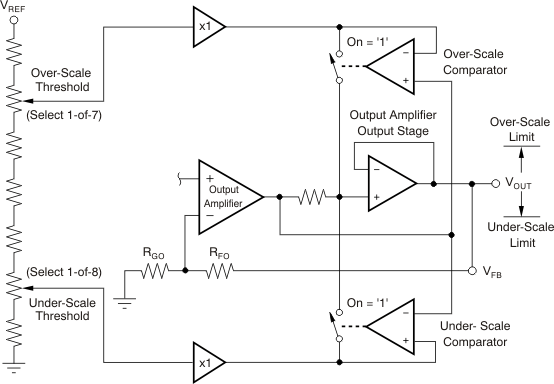
The Over-Scale and Under-Scale Limit circuit provides a programmable upper and lower clip limit for the PGA309 output voltage. This circuit can be enabled by setting Register 5, bit D6 to ‘1’. When combined with the Fault Monitor circuitry, system diagnostics can be performed to determine if a conditioned sensor is defective or if the process being monitored by the sensor is out of range. Figure 2-24 details the key sections of the Over-Scale and Under-Scale Limit circuit. The selected PGA309 VREF is divided down by a precision resistor string to form the over-scale and under-scale thresholds, as shown in Table 2-18 and Table 2-19. Register 5 bits [5:0] set the desired thresholds. These resistor ratios are extremely accurate and produce no significant initial or temperature errors. As shown in Figure 2-24, there are two separate comparators: over-scale and under-scale, which use the over-scale or under-scale threshold, respectively, and determine where the PGA309 output (VOUT) will be clipped. The dominant errors in the Over-Scale and Under-Scale Limit circuit are due to the comparators offset and offset temperature drift.
 Figure 2-24 Over-Scale and Under-Scale Limit Circuit
| HL2 [5] |
HL1 [4] |
HL0 [3] |
Over-Scale Threshold (V) |
Over-Scale Threshold |
|---|---|---|---|---|
| 0 | 0 | 0 | 4.854 | 0.9708 VREF |
| 0 | 0 | 1 | 4.805 | 0.9610 VREF |
| 0 | 1 | 0 | 4.698 | 0.9394 VREF |
| 0 | 1 | 1 | 4.580 | 0.9160 VREF |
| 1 | 0 | 0 | 4.551 | 0.9102 VREF |
| 1 | 0 | 1 | 3.662 | 0.7324 VREF |
| 1 | 1 | 0 | 2.764 | 0.5528 VREF |
| 1 | 1 | 1 | Reserved | — |
| LL2 [2] |
LL1 [1] |
LL0 [0] |
Under-Scale Threshold (V) |
Under-Scale Threshold |
|---|---|---|---|---|
| 0 | 0 | 0 | 0.127 | 0.02540 VREF |
| 0 | 0 | 1 | 0.147 | 0.02930 VREF |
| 0 | 1 | 0 | 0.176 | 0.03516 VREF |
| 0 | 1 | 1 | 0.196 | 0.03906 VREF |
| 1 | 0 | 0 | 0.225 | 0.04492 VREF |
| 1 | 0 | 1 | 0.254 | 0.05078 VREF |
| 1 | 1 | 0 | 0.274 | 0.05468 VREF |
| 1 | 1 | 1 | 0.303 | 0.06054 VREF |
The design considerations in using the Over-Scale and Under-Scale Limit circuit are best understood through a definition by example, as shown in Example2-4.