SBOU024C august 2004 – july 2023 PGA309
- 1
- Read This First
-
1Introduction
- 1.1 PGA309 Functional Description
- 1.2 Sensor Error Adjustment Range
- 1.3 Gain Scaling
- 1.4 Offset Adjustment
- 1.5 Voltage Reference
- 1.6 Sensor Excitation and Linearization
- 1.7 ADC for Temperature Sensing
- 1.8 External EEPROM and Temperature Coefficients
- 1.9 Fault Monitor
- 1.10 Over-Scale and Under-Scale Limits
- 1.11 Power-Up and Normal Operation
- 1.12 Digital Interface
- 1.13 Pin Configuration
- 2Detailed Description
- 3Operating Modes
-
4Digital Interface
- 4.1 Description
- 4.2 Two-Wire Interface
- 4.3 One-Wire Interface
- 4.4 One-Wire Interface Timeout
- 4.5 One-Wire Interface Timing Considerations
- 4.6 Two-Wire Access to External EEPROM
- 4.7 One-Wire Interface Initiated Two-Wire EEPROM Transactions
- 4.8 PGA309 Stand-Alone Mode and Two-Wire Transactions
- 4.9 PGA309 Two-Wire Bus Master Operation and Bus Sharing Considerations
- 4.10 One-Wire Operation with PRG Connected to VOUT
- 4.11 Four-Wire Modules and One-Wire Interface (PRG)
- 5Application Background
-
6Register Descriptions
- 6.1 Internal Register Overview
- 6.2
Internal Register Map
- 6.2.1 Register 0: Temp ADC Output Register (Read Only, Address Pointer = 00000)
- 6.2.2 Register 1: Fine Offset Adjust (Zero DAC) Register (Read/Write, Address Pointer = 00001)
- 6.2.3 Register 2: Fine Gain Adjust (Gain DAC) Register (Read/Write, Address Pointer = 00010)
- 6.2.4 Register 3: Reference Control and Linearization Register (Read/Write, Address Pointer = 00011)
- 6.2.5 Register 4: PGA Coarse Offset Adjust and Gain Select/Output Amplifier Gain Select Register (Read/Write, Address Pointer = 00100)
- 6.2.6 Register 5: PGA Configuration and Over/Under-Scale Limit Register (Read/Write, Address Pointer = 00101)
- 6.2.7 Register 6: Temp ADC Control Register (Read/Write, Address Pointer = 00110)
- 6.2.8 Register 7: Output Enable Counter Control Register (Read/Write, Address Pointer = 00111)
- 6.2.9 Register 8: Alarm Status Register (Read Only, Address Pointer = 01000)
- A External EEPROM Example
- B Detailed Block Diagram
- C Glossary
- Revision History
4.9 PGA309 Two-Wire Bus Master Operation and Bus Sharing Considerations
Whenever the PGA309 is called upon to communicate to the external EEPROM, the PGA309 must become the master on the Two-Wire interface bus. In order to do this in a reliable and orderly fashion, the PGA309 contains fault diagnostics to attempt to free a stuck bus. Several monitors and algorithms check for bus availability, prevent bus contention in case other devices are connected in parallel with the External EEPROM.
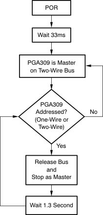
If the PGA309 is ever addressed on its Two-Wire or One-Wire interface, with the PGA309 providing a successful acknowledge, the PGA309 will cease all transactions as a master on the Two-Wire bus and give up control for 1.3 seconds. Each time the PGA309 is addressed on the Two-Wire bus, the 1.3 second timeout is reset, as shown in Figure 4-13.
 Figure 4-13 Two-Wire Bus Relinquish by PGA309 in Master Mode
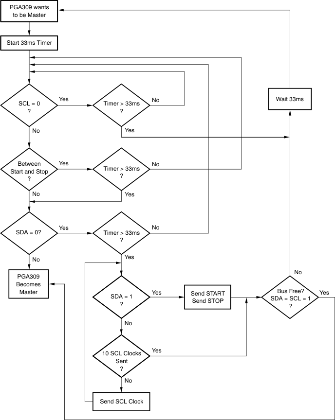
Figure 4-14 details the algorithms used by the PGA309 when it must become master on the Two-Wire bus. A 33ms timer is started. Now SCL is monitored for being low. If SCL is not low, the PGA309 checks to see if communication on the Two-Wire bus is between a START and a STOP. If the bus communication is between a START and a STOP, the PGA309 waits for the 33ms timer to time out, and then checks if SDA is low. If SDA is not low and SCL is high, the PGA309 becomes bus master. If there is any SCL activity during the 33ms interval, the 33ms timer will restart.
 Figure 4-14 Two-Wire Bus Master Algorithm
If SCL remains low for the entire 33ms timer countdown, the PGA309 waits 33ms before starting the 33ms timer again to begin to check the bus for an idle state (SDA = SCL = ‘1’).
If SDA is low after the 33ms timer counts down, the PGA309 interprets this as a stuck-bus condition. The PGA309 attempts to free the stuck bus by sending up to ten clocks down SCL to free up SDA. If it is successful in causing SDA to go high, the PGA309 sends a START and then STOP sequence to ensure a complete reset of whichever device was causing the stuck bus. Now the bus should be in an idle state (SDA = SCL = ‘1’) and the PGA309 can become the master on the bus.
If the PGA309 is communicating on the bus as a master and it sees contention, the PGA309 will release the bus and retry in 33ms. Contention is defined as the PGA309 wanting SCL high and SCL is low, or wanting SDA high and SDA is low.