SBOU024C august 2004 – july 2023 PGA309
- 1
- Read This First
-
1Introduction
- 1.1 PGA309 Functional Description
- 1.2 Sensor Error Adjustment Range
- 1.3 Gain Scaling
- 1.4 Offset Adjustment
- 1.5 Voltage Reference
- 1.6 Sensor Excitation and Linearization
- 1.7 ADC for Temperature Sensing
- 1.8 External EEPROM and Temperature Coefficients
- 1.9 Fault Monitor
- 1.10 Over-Scale and Under-Scale Limits
- 1.11 Power-Up and Normal Operation
- 1.12 Digital Interface
- 1.13 Pin Configuration
- 2Detailed Description
- 3Operating Modes
-
4Digital Interface
- 4.1 Description
- 4.2 Two-Wire Interface
- 4.3 One-Wire Interface
- 4.4 One-Wire Interface Timeout
- 4.5 One-Wire Interface Timing Considerations
- 4.6 Two-Wire Access to External EEPROM
- 4.7 One-Wire Interface Initiated Two-Wire EEPROM Transactions
- 4.8 PGA309 Stand-Alone Mode and Two-Wire Transactions
- 4.9 PGA309 Two-Wire Bus Master Operation and Bus Sharing Considerations
- 4.10 One-Wire Operation with PRG Connected to VOUT
- 4.11 Four-Wire Modules and One-Wire Interface (PRG)
- 5Application Background
-
6Register Descriptions
- 6.1 Internal Register Overview
- 6.2
Internal Register Map
- 6.2.1 Register 0: Temp ADC Output Register (Read Only, Address Pointer = 00000)
- 6.2.2 Register 1: Fine Offset Adjust (Zero DAC) Register (Read/Write, Address Pointer = 00001)
- 6.2.3 Register 2: Fine Gain Adjust (Gain DAC) Register (Read/Write, Address Pointer = 00010)
- 6.2.4 Register 3: Reference Control and Linearization Register (Read/Write, Address Pointer = 00011)
- 6.2.5 Register 4: PGA Coarse Offset Adjust and Gain Select/Output Amplifier Gain Select Register (Read/Write, Address Pointer = 00100)
- 6.2.6 Register 5: PGA Configuration and Over/Under-Scale Limit Register (Read/Write, Address Pointer = 00101)
- 6.2.7 Register 6: Temp ADC Control Register (Read/Write, Address Pointer = 00110)
- 6.2.8 Register 7: Output Enable Counter Control Register (Read/Write, Address Pointer = 00111)
- 6.2.9 Register 8: Alarm Status Register (Read Only, Address Pointer = 01000)
- A External EEPROM Example
- B Detailed Block Diagram
- C Glossary
- Revision History

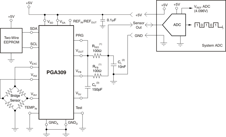
(Although not needed in all applications):
Figure 2-25 Absolute Scale System—PGA309 Connected to a System ADC- RISO and RFB provide the PGA309 with overvoltage protection on Sensor Out.
- CL provides EMI/RFI filtering.
- CF provides the PGA309 with stability for capacitive load of CL.
Table 2-20 Electrical Characteristics for Over-Scale and Under-Scale Comparators and VREF
| Parameter | Min | Typ | Max | Units |
|---|---|---|---|---|
| Over-Scale Comparator Offset | +6 | +60 | +114 | mV |
| Over-Scale Comparator Offset Drift | +0.37 | mV/°C | ||
| Under-Scale Comparator Offset | −7 | −50 | −93 | mV |
| Under-Scale Comparator Offset Drift | −0.15 | mV/°C | ||
| VREF2 | 4.00 | 4.096 | 4.14 | V |
| VREF2 Drift | +10 | ppm/°C |
Table 2-21 Over-Scale and Under-Scale Min and Max Trip Point Calculations(1)
| Threshold U = Under-Scale O = Over-Scale |
Threshold Ratio to VREF |
Min Trip (V) |
Min Trip (%VREF ADC) |
Max Trip (V) |
Max Trip (%VREF ADC) |
Typ Trip (V) |
Typ Trip (%VREF ADC) |
|---|---|---|---|---|---|---|---|
| U7 | 0.0605 | 0.1338 | 3.2656 | 0.2483 | 6.0616 | 0.1910 | 4.6636 |
| U6 | 0.0547 | 0.1104 | 2.6943 | 0.2240 | 5.4684 | 0.1672 | 4.0814 |
| U5 | 0.0508 | 0.0948 | 2.3141 | 0.2078 | 5.0736 | 0.1513 | 3.6938 |
| U4 | 0.0449 | 0.0714 | 1.7428 | 0.1835 | 4.4804 | 0.1274 | 3.1116 |
| U3 | 0.0391 | 0.0480 | 1.1714 | 0.1592 | 3.8871 | 0.1036 | 2.5293 |
| U2 | 0.0352 | 0.0324 | 0.7912 | 0.1430 | 3.4923 | 0.0877 | 2.1418 |
| U1 | 0.0293 | 0.0090 | 0.2199 | 0.1187 | 2.8991 | 0.0639 | 1.5595 |
| U0 | 0.0254 | −0.0066 | −0.1603 | 0.1026 | 2.5042 | 0.0480 | 1.1719 |
| O6 | 0.5528 | 2.1895 | 53.4546 | 2.4432 | 59.6494 | 2.3164 | 56.5520 |
| O5 | 0.7324 | 2.9067 | 70.9648 | 3.1880 | 77.8313 | 3.0473 | 74.3980 |
| O4 | 0.9102 | 3.6167 | 88.2994 | 3.9252 | 95.8309 | 3.7710 | 92.0652 |
| O3 | 0.9160 | 3.6399 | 88.8649 | 3.9493 | 96.4181 | 3.7946 | 92.6415 |
| O2 | 0.9394 | 3.7333 | 91.1462 | 4.0463 | 98.7870 | 3.8898 | 94.9666 |
| O1 | 0.9610 | 3.8196 | 93.2521 | 4.1359 | 100.9737 | 3.9777 | 97.1129 |
| O0 | 0.9708 | 3.8587 | 94.2076 | 4.1765 | 101.9658 | 4.0176 | 98.0867 |
(1) VREF MIN = 3.9934V, VREF MAX = 4.1466V, VREF ADC = 4.096V, VOS min = −0.01805V, VOS max = 0.151V,
VUS min = −0.00275V, VUS max = −0.108V. Bold Italics indicate final choice for Example2-4.
VUS min = −0.00275V, VUS max = −0.108V. Bold Italics indicate final choice for Example2-4.
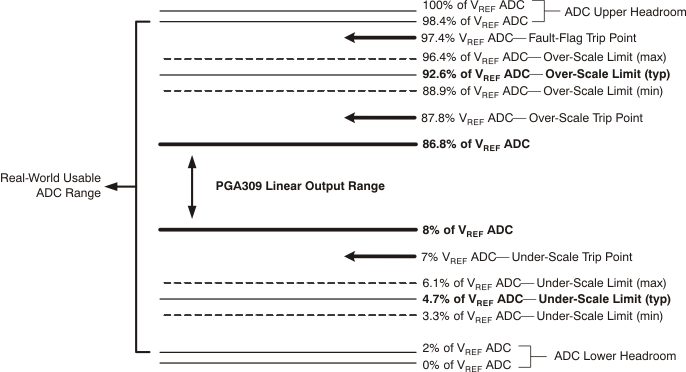
 Figure 2-26 System ADC Range Budget for Over-Scale, Under-Scale, and Linear Output
Table 2-22 PGA309 VOUT Limits for System ADC Range Budget(1)
| Limiting Condition | PGA309 VOUT (V) | PGA309 VOUT Limit (V) |
|---|---|---|
| 96.4% VREF ADC—Over-Scale Limit (max) | 3.9493 | 4.9 |
| 3.3% VREF ADC—Under-Scale Limit (min) | 0.1338 | 0.1 |
(1) VREF ADC = 4.096V, VSA = 5V.