SBAS813 June 2018 ADS8688AT
PRODUCTION DATA.
- 1 Features
- 2 Applications
- 3 Description
- 4 Revision History
- 5 Pin Configuration and Functions
- 6 Specifications
-
7 Detailed Description
- 7.1 Overview
- 7.2 Functional Block Diagram
- 7.3
Feature Description
- 7.3.1 Analog Inputs
- 7.3.2 Analog Input Impedance
- 7.3.3 Input Overvoltage Protection Circuit
- 7.3.4 Programmable Gain Amplifier (PGA)
- 7.3.5 Second-Order, Low-Pass Filter (LPF)
- 7.3.6 ADC Driver
- 7.3.7 Multiplexer (MUX)
- 7.3.8 Reference
- 7.3.9 Auxiliary Channel
- 7.3.10 ADC Transfer Function
- 7.3.11 Alarm Feature
- 7.4
Device Functional Modes
- 7.4.1 Device Interface
- 7.4.2
Device Modes
- 7.4.2.1 Continued Operation in the Selected Mode (NO_OP)
- 7.4.2.2 Frame Abort Condition (FRAME_ABORT)
- 7.4.2.3 STANDBY Mode (STDBY)
- 7.4.2.4 Power-Down Mode (PWR_DN)
- 7.4.2.5 Auto Channel Enable With Reset (AUTO_RST)
- 7.4.2.6 Manual Channel n Select (MAN_Ch_n)
- 7.4.2.7 Channel Sequencing Modes
- 7.4.2.8 Reset Program Registers (RST)
- 7.5
Register Maps
- 7.5.1 Command Register Description
- 7.5.2
Program Register Description
- 7.5.2.1 Program Register Read/Write Operation
- 7.5.2.2 Program Register Map
- 7.5.2.3
Program Register Descriptions
- 7.5.2.3.1 Auto-Scan Sequencing Control Registers
- 7.5.2.3.2 Device Features Selection Control Register (address = 03h)
- 7.5.2.3.3 Range Select Registers (addresses 05h-0Ch)
- 7.5.2.3.4 Alarm Flag Registers (Read-Only)
- 7.5.2.3.5
Alarm Threshold Setting Registers
- Table 22. Channel n Hysteresis Register Field Descriptions (n = 0 to 7)
- Table 23. Channel n High Threshold MSB Register Field Descriptions (n = 0 to 7)
- Table 24. Channel n High Threshold LSB Register Field Descriptions (n = 0 to 7)
- Table 25. Channel n Low Threshold MSB Register Field Descriptions (n = 0 to 7)
- Table 26. Channel n Low Threshold MSB Register Field Descriptions (n = 0 to 7)
- 7.5.2.3.6 Command Read-Back Register (address = 3Fh)
- 8 Application and Implementation
- 9 Power Supply Recommendations
- 10Layout
- 11Device and Documentation Support
- 12Mechanical, Packaging, and Orderable Information
Package Options
Mechanical Data (Package|Pins)
- DBT|38
Thermal pad, mechanical data (Package|Pins)
Orderable Information
7.3.11 Alarm Feature
The device has an active-high ALARM output on pin 35. The ALARM signal is synchronous and changes its state on the 16th falling edge of the SCLK signal. A high level on ALARM indicates that the alarm flag has tripped on one or more channels of the device. This pin can be wired to interrupt the host input. When an ALARM interrupt is received, the alarm flag registers are read to determine which channels have an alarm. The device features independently programmable alarms for each channel. There are two alarms per channel (a low and a high alarm) and each alarm threshold has a separate hysteresis setting.
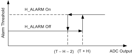
The ADS8688AT sets a high alarm when the digital output for a particular channel exceeds the high alarm upper limit [high alarm threshold (T) + hysteresis (H)]. The alarm resets when the digital output for the channel is less than or equal to the high alarm lower limit (high alarm T – H – 2). Figure 82 shows this function.
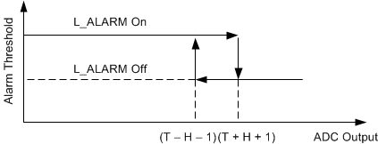
Similarly, the lower alarm is triggered when the digital output for a particular channel falls below the low alarm lower limit (low alarm threshold T – H – 1). The alarm resets when the digital output for the channel is greater than or equal to the low alarm higher limit (low alarm T + H + 1). Figure 83 shows this function.
 Figure 82. High-ALARM Hysteresis
 Figure 83. Low-ALARM Hysteresis
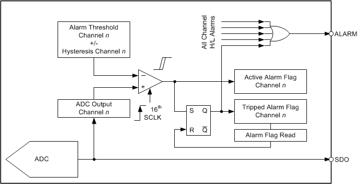
Figure 84 depicts a functional block diagram for a single-channel alarm. There are two flags for each high and low alarm: active alarm flag and tripped alarm flag; see the alarm flag registers for more details. The active alarm flag is triggered when an alarm condition is encountered for a particular channel; the active alarm flag resets when the alarm shuts off. A tripped alarm flag sets an alarm condition in the same manner as for an active alarm flag. However, the tripped alarm flag remains latched and resets only when the appropriate alarm flag register is read.
 Figure 84. Alarm Functionality Schematic