SBAS813 June 2018 ADS8688AT
PRODUCTION DATA.
- 1 Features
- 2 Applications
- 3 Description
- 4 Revision History
- 5 Pin Configuration and Functions
- 6 Specifications
-
7 Detailed Description
- 7.1 Overview
- 7.2 Functional Block Diagram
- 7.3
Feature Description
- 7.3.1 Analog Inputs
- 7.3.2 Analog Input Impedance
- 7.3.3 Input Overvoltage Protection Circuit
- 7.3.4 Programmable Gain Amplifier (PGA)
- 7.3.5 Second-Order, Low-Pass Filter (LPF)
- 7.3.6 ADC Driver
- 7.3.7 Multiplexer (MUX)
- 7.3.8 Reference
- 7.3.9 Auxiliary Channel
- 7.3.10 ADC Transfer Function
- 7.3.11 Alarm Feature
- 7.4
Device Functional Modes
- 7.4.1 Device Interface
- 7.4.2
Device Modes
- 7.4.2.1 Continued Operation in the Selected Mode (NO_OP)
- 7.4.2.2 Frame Abort Condition (FRAME_ABORT)
- 7.4.2.3 STANDBY Mode (STDBY)
- 7.4.2.4 Power-Down Mode (PWR_DN)
- 7.4.2.5 Auto Channel Enable With Reset (AUTO_RST)
- 7.4.2.6 Manual Channel n Select (MAN_Ch_n)
- 7.4.2.7 Channel Sequencing Modes
- 7.4.2.8 Reset Program Registers (RST)
- 7.5
Register Maps
- 7.5.1 Command Register Description
- 7.5.2
Program Register Description
- 7.5.2.1 Program Register Read/Write Operation
- 7.5.2.2 Program Register Map
- 7.5.2.3
Program Register Descriptions
- 7.5.2.3.1 Auto-Scan Sequencing Control Registers
- 7.5.2.3.2 Device Features Selection Control Register (address = 03h)
- 7.5.2.3.3 Range Select Registers (addresses 05h-0Ch)
- 7.5.2.3.4 Alarm Flag Registers (Read-Only)
- 7.5.2.3.5
Alarm Threshold Setting Registers
- Table 22. Channel n Hysteresis Register Field Descriptions (n = 0 to 7)
- Table 23. Channel n High Threshold MSB Register Field Descriptions (n = 0 to 7)
- Table 24. Channel n High Threshold LSB Register Field Descriptions (n = 0 to 7)
- Table 25. Channel n Low Threshold MSB Register Field Descriptions (n = 0 to 7)
- Table 26. Channel n Low Threshold MSB Register Field Descriptions (n = 0 to 7)
- 7.5.2.3.6 Command Read-Back Register (address = 3Fh)
- 8 Application and Implementation
- 9 Power Supply Recommendations
- 10Layout
- 11Device and Documentation Support
- 12Mechanical, Packaging, and Orderable Information
Package Options
Mechanical Data (Package|Pins)
- DBT|38
Thermal pad, mechanical data (Package|Pins)
Orderable Information
7.4.2.5 Auto Channel Enable With Reset (AUTO_RST)
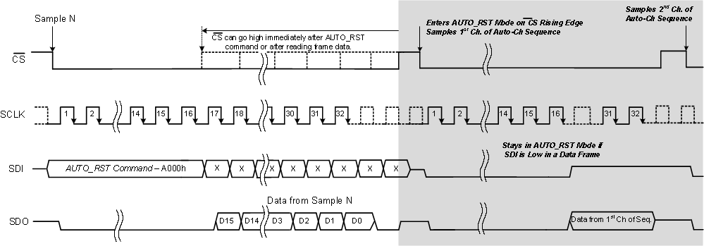
The device can be programmed as explained in Figure 96 to scan the input signal on all analog channels automatically by writing a valid auto channel sequence with a reset (AUTO_RST, A000h) command in the command register. As shown in Figure 96, the CS signal can be pulled high immediately after the AUTO_RST command or after reading the output data of the frame. However, in order to accurately acquire and convert the input signal on the first selected channel in the next data frame, the command frame must be a complete frame of 32 SCLK cycles.
The sequence of channels for the automatic scan can be configured by the AUTO SCAN sequencing control register (01h to 02h) in the program register; see the Program Register Map section. In this mode, the device continuously cycles through the selected channels in ascending order, beginning with the lowest channel and converting all channels selected in the program register. On completion of the sequence, the device returns to the lowest count channel in the program register and repeats the sequence. The input voltage range for each channel in the auto-scan sequence can be configured by setting the range select registers of the program registers.
 Figure 96. Enter AUTO_RST Mode Timing Diagram
The device remains in AUTO_RST mode if no other valid command is executed and SDI is kept low (see the Continued Operation in the Selected Mode (NO_OP) section) during subsequent data frames. If the AUTO_RST command is executed again at any time during this mode of operation, then the sequence of the scanned channels is reset. The device returns to the lowest count channel of the auto-scan sequence in the program register and repeats the sequence. The timing diagram in Figure 97 shows this behavior using an example in which channels 0 to 2 are selected in the auto sequence. For switching between AUTO_RST mode and MAN_Ch_n mode; see the Channel Sequencing Modes section.
 Figure 97. Device Operation Example in AUTO_RST Mode