SBAS813 June 2018 ADS8688AT
PRODUCTION DATA.
- 1 Features
- 2 Applications
- 3 Description
- 4 Revision History
- 5 Pin Configuration and Functions
- 6 Specifications
-
7 Detailed Description
- 7.1 Overview
- 7.2 Functional Block Diagram
- 7.3
Feature Description
- 7.3.1 Analog Inputs
- 7.3.2 Analog Input Impedance
- 7.3.3 Input Overvoltage Protection Circuit
- 7.3.4 Programmable Gain Amplifier (PGA)
- 7.3.5 Second-Order, Low-Pass Filter (LPF)
- 7.3.6 ADC Driver
- 7.3.7 Multiplexer (MUX)
- 7.3.8 Reference
- 7.3.9 Auxiliary Channel
- 7.3.10 ADC Transfer Function
- 7.3.11 Alarm Feature
- 7.4
Device Functional Modes
- 7.4.1 Device Interface
- 7.4.2
Device Modes
- 7.4.2.1 Continued Operation in the Selected Mode (NO_OP)
- 7.4.2.2 Frame Abort Condition (FRAME_ABORT)
- 7.4.2.3 STANDBY Mode (STDBY)
- 7.4.2.4 Power-Down Mode (PWR_DN)
- 7.4.2.5 Auto Channel Enable With Reset (AUTO_RST)
- 7.4.2.6 Manual Channel n Select (MAN_Ch_n)
- 7.4.2.7 Channel Sequencing Modes
- 7.4.2.8 Reset Program Registers (RST)
- 7.5
Register Maps
- 7.5.1 Command Register Description
- 7.5.2
Program Register Description
- 7.5.2.1 Program Register Read/Write Operation
- 7.5.2.2 Program Register Map
- 7.5.2.3
Program Register Descriptions
- 7.5.2.3.1 Auto-Scan Sequencing Control Registers
- 7.5.2.3.2 Device Features Selection Control Register (address = 03h)
- 7.5.2.3.3 Range Select Registers (addresses 05h-0Ch)
- 7.5.2.3.4 Alarm Flag Registers (Read-Only)
- 7.5.2.3.5
Alarm Threshold Setting Registers
- Table 22. Channel n Hysteresis Register Field Descriptions (n = 0 to 7)
- Table 23. Channel n High Threshold MSB Register Field Descriptions (n = 0 to 7)
- Table 24. Channel n High Threshold LSB Register Field Descriptions (n = 0 to 7)
- Table 25. Channel n Low Threshold MSB Register Field Descriptions (n = 0 to 7)
- Table 26. Channel n Low Threshold MSB Register Field Descriptions (n = 0 to 7)
- 7.5.2.3.6 Command Read-Back Register (address = 3Fh)
- 8 Application and Implementation
- 9 Power Supply Recommendations
- 10Layout
- 11Device and Documentation Support
- 12Mechanical, Packaging, and Orderable Information
Package Options
Mechanical Data (Package|Pins)
- DBT|38
Thermal pad, mechanical data (Package|Pins)
Orderable Information
7.3.3 Input Overvoltage Protection Circuit
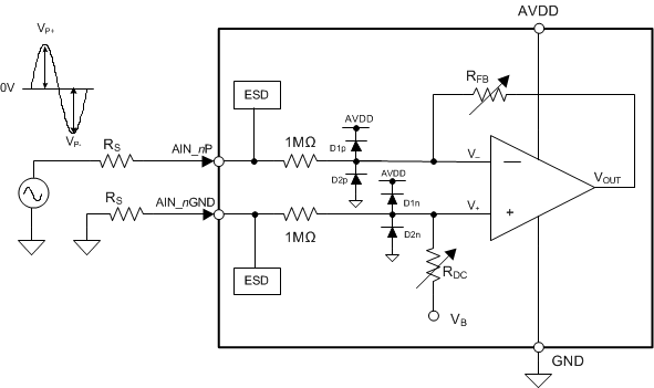
The ADS8688AT features an internal overvoltage protection circuit on each of the eight analog input channels. Use these protection circuits as a secondary protection scheme to protect the device. Using external protection devices against surges, electrostatic discharge (ESD), and electrical fast transient (EFT) conditions is highly recommended. Figure 66 shows the conceptual block diagram of the internal overvoltage protection (OVP) circuit.
 Figure 66. Input Overvoltage Protection Circuit Schematic
As shown in Figure 66, the combination of the 1-MΩ input resistors along with the PGA gain-setting resistors (RFB and RDC) limit the current flowing into the input pins. A combination of antiparallel diodes (D1 and D2) are added on each input pin to protect the internal circuitry and set the overvoltage protection limits.
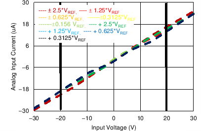
Table 1 explains the various operating conditions for the device when the device is powered on. Table 1 indicates that when the AVDD pin of the device is connected to the proper supply voltage (AVDD = 5 V), the internal overvoltage protection circuit can withstand up to ±20 V on the analog input pins.
Table 1. Input Overvoltage Protection Limits When AVDD = 5 V(1)
| INPUT CONDITION
(VOVP = ±20 V) |
TEST CONDITION | ADC OUTPUT | COMMENTS | |
|---|---|---|---|---|
| |VIN| < |VRANGE| | Within operating range | All input ranges | Valid | Device functions as per data sheet specifications |
| |VRANGE| < |VIN| < |VOVP| | Beyond operating range but within overvoltage range | All input ranges | Saturated | ADC output is saturated, but device is internally protected (not recommended for extended time) |
| |VIN| > |VOVP| | Beyond overvoltage range | All input ranges | Saturated | This usage condition may cause irreversible damage to the device |
The results indicated in Table 1 are based on an assumption that the analog input pins are driven by very low impedance sources (RS is approximately 0 Ω). However, if the sources driving the inputs have higher impedance, the current flowing through the protection diodes reduces further, thereby increasing the OVP voltage range. Higher source impedance results in gain errors and contributes to overall system noise performance.
Figure 67 shows the voltage versus current response of the internal overvoltage protection circuit when the device is powered on. According to this current-to-voltage (I-V) response, the current flowing into the device input pins is limited by the 1-MΩ input impedance. However, for voltages beyond ±20 V, the internal node voltages surpass the break-down voltage for internal transistors, thus setting the limit for overvoltage protection on the input pins.
The same overvoltage protection circuit also provides protection to the device when the device is not powered on and AVDD is floating. This condition can arise when the input signals are applied before the ADC is fully powered on. Table 2 lists the overvoltage protection limits for this condition.
Table 2. Input Overvoltage Protection Limits When AVDD = Floating(1)
| INPUT CONDITION
(VOVP = ±11 V) |
TEST CONDITION | ADC OUTPUT | COMMENTS | |
|---|---|---|---|---|
| |VIN| < |VOVP| | Within overvoltage range | All input ranges | Invalid | Device is not functional but is protected internally by the OVP circuit |
| |VIN| > |VOVP| | Beyond overvoltage range | All input ranges | Invalid | This usage condition may cause irreversible damage to the device |
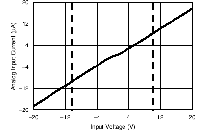
Figure 68 shows the voltage versus current response of the internal overvoltage protection circuit when the device is not powered on. According to this I-V response, the current flowing into the device input pins is limited by the 1-MΩ input impedance. However, for voltages beyond ±11 V, the internal node voltages surpass the break-down voltage for internal transistors, thus setting the limit for overvoltage protection on the input pins.
 Figure 67. I-V Curve for an Input OVP Circuit
 Figure 68. I-V Curve for an Input OVP Circuit
(AVDD = Floating)