SBAS813 June 2018 ADS8688AT
PRODUCTION DATA.
- 1 Features
- 2 Applications
- 3 Description
- 4 Revision History
- 5 Pin Configuration and Functions
- 6 Specifications
-
7 Detailed Description
- 7.1 Overview
- 7.2 Functional Block Diagram
- 7.3
Feature Description
- 7.3.1 Analog Inputs
- 7.3.2 Analog Input Impedance
- 7.3.3 Input Overvoltage Protection Circuit
- 7.3.4 Programmable Gain Amplifier (PGA)
- 7.3.5 Second-Order, Low-Pass Filter (LPF)
- 7.3.6 ADC Driver
- 7.3.7 Multiplexer (MUX)
- 7.3.8 Reference
- 7.3.9 Auxiliary Channel
- 7.3.10 ADC Transfer Function
- 7.3.11 Alarm Feature
- 7.4
Device Functional Modes
- 7.4.1 Device Interface
- 7.4.2
Device Modes
- 7.4.2.1 Continued Operation in the Selected Mode (NO_OP)
- 7.4.2.2 Frame Abort Condition (FRAME_ABORT)
- 7.4.2.3 STANDBY Mode (STDBY)
- 7.4.2.4 Power-Down Mode (PWR_DN)
- 7.4.2.5 Auto Channel Enable With Reset (AUTO_RST)
- 7.4.2.6 Manual Channel n Select (MAN_Ch_n)
- 7.4.2.7 Channel Sequencing Modes
- 7.4.2.8 Reset Program Registers (RST)
- 7.5
Register Maps
- 7.5.1 Command Register Description
- 7.5.2
Program Register Description
- 7.5.2.1 Program Register Read/Write Operation
- 7.5.2.2 Program Register Map
- 7.5.2.3
Program Register Descriptions
- 7.5.2.3.1 Auto-Scan Sequencing Control Registers
- 7.5.2.3.2 Device Features Selection Control Register (address = 03h)
- 7.5.2.3.3 Range Select Registers (addresses 05h-0Ch)
- 7.5.2.3.4 Alarm Flag Registers (Read-Only)
- 7.5.2.3.5
Alarm Threshold Setting Registers
- Table 22. Channel n Hysteresis Register Field Descriptions (n = 0 to 7)
- Table 23. Channel n High Threshold MSB Register Field Descriptions (n = 0 to 7)
- Table 24. Channel n High Threshold LSB Register Field Descriptions (n = 0 to 7)
- Table 25. Channel n Low Threshold MSB Register Field Descriptions (n = 0 to 7)
- Table 26. Channel n Low Threshold MSB Register Field Descriptions (n = 0 to 7)
- 7.5.2.3.6 Command Read-Back Register (address = 3Fh)
- 8 Application and Implementation
- 9 Power Supply Recommendations
- 10Layout
- 11Device and Documentation Support
- 12Mechanical, Packaging, and Orderable Information
Package Options
Mechanical Data (Package|Pins)
- DBT|38
Thermal pad, mechanical data (Package|Pins)
Orderable Information
8.2.1.3 Application Curve
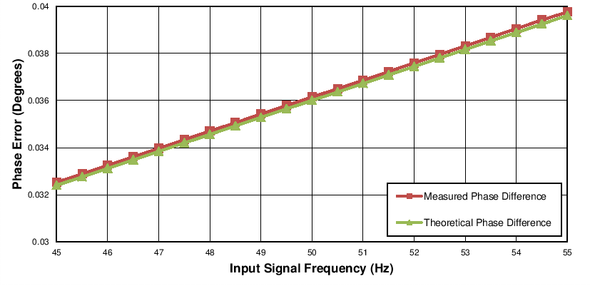
Table 28 and Figure 121 summarize the performance for this design. In this example, multiple sinusoidal input signals of an amplitude at ±10 V are applied to the inputs of the ADC. The initial phase angle is the same for all signals, but the input frequency is varied from 45 Hz to 55 Hz. The phase error in the last column of Table 28 reflects the measurement accuracy of this design.
Table 28. Theoretical and Measured Phase Difference
| INPUT TEST CONDITION | THEORETICAL PHASE ERROR(1) | MEASURED PHASE ERROR(2) | PHASE ERROR AFTER COMPENSATION(3) |
|---|---|---|---|
| Phase difference
(consecutive channels) |
0.036° | 0.036145° | 0.000145° |
| Phase difference
(farthest channels, channel 0 to channel 7) |
0.252° | 0.249964° | 0.002036° |
(1) Theoretical phase difference introduced by multiplexing is calculated based on the formula: Δφ = (fIN / fADC) × N × 360°, where N = integral gap between two channels in the multiplexer sequence; fIN = input signal frequency; and fADC = 500 kSPS, maximum throughput of the ADC.
(2) Measured phase value (before compensation) includes phase difference between any two channels resulting from multiplexing ADC inputs.
(3) The algorithm subtracts theoretical phase difference from the measured phase to compensate for the phase difference resulting from the MUX inputs.
 Figure 121. Measured and Theoretical Phase Difference Between Consecutive Channels

|
For a step-by-step design procedure, circuit schematics, bill of materials, PCB files, simulation results, and test results, see Phase Compensated 8-Channel, Multiplexed Data Acquisition System for Power Automation Reference Design. |