SBAS813 June 2018 ADS8688AT
PRODUCTION DATA.
- 1 Features
- 2 Applications
- 3 Description
- 4 Revision History
- 5 Pin Configuration and Functions
- 6 Specifications
-
7 Detailed Description
- 7.1 Overview
- 7.2 Functional Block Diagram
- 7.3
Feature Description
- 7.3.1 Analog Inputs
- 7.3.2 Analog Input Impedance
- 7.3.3 Input Overvoltage Protection Circuit
- 7.3.4 Programmable Gain Amplifier (PGA)
- 7.3.5 Second-Order, Low-Pass Filter (LPF)
- 7.3.6 ADC Driver
- 7.3.7 Multiplexer (MUX)
- 7.3.8 Reference
- 7.3.9 Auxiliary Channel
- 7.3.10 ADC Transfer Function
- 7.3.11 Alarm Feature
- 7.4
Device Functional Modes
- 7.4.1 Device Interface
- 7.4.2
Device Modes
- 7.4.2.1 Continued Operation in the Selected Mode (NO_OP)
- 7.4.2.2 Frame Abort Condition (FRAME_ABORT)
- 7.4.2.3 STANDBY Mode (STDBY)
- 7.4.2.4 Power-Down Mode (PWR_DN)
- 7.4.2.5 Auto Channel Enable With Reset (AUTO_RST)
- 7.4.2.6 Manual Channel n Select (MAN_Ch_n)
- 7.4.2.7 Channel Sequencing Modes
- 7.4.2.8 Reset Program Registers (RST)
- 7.5
Register Maps
- 7.5.1 Command Register Description
- 7.5.2
Program Register Description
- 7.5.2.1 Program Register Read/Write Operation
- 7.5.2.2 Program Register Map
- 7.5.2.3
Program Register Descriptions
- 7.5.2.3.1 Auto-Scan Sequencing Control Registers
- 7.5.2.3.2 Device Features Selection Control Register (address = 03h)
- 7.5.2.3.3 Range Select Registers (addresses 05h-0Ch)
- 7.5.2.3.4 Alarm Flag Registers (Read-Only)
- 7.5.2.3.5
Alarm Threshold Setting Registers
- Table 22. Channel n Hysteresis Register Field Descriptions (n = 0 to 7)
- Table 23. Channel n High Threshold MSB Register Field Descriptions (n = 0 to 7)
- Table 24. Channel n High Threshold LSB Register Field Descriptions (n = 0 to 7)
- Table 25. Channel n Low Threshold MSB Register Field Descriptions (n = 0 to 7)
- Table 26. Channel n Low Threshold MSB Register Field Descriptions (n = 0 to 7)
- 7.5.2.3.6 Command Read-Back Register (address = 3Fh)
- 8 Application and Implementation
- 9 Power Supply Recommendations
- 10Layout
- 11Device and Documentation Support
- 12Mechanical, Packaging, and Orderable Information
Package Options
Mechanical Data (Package|Pins)
- DBT|38
Thermal pad, mechanical data (Package|Pins)
Orderable Information
7.3.8.1 Internal Reference
The device has an internal 4.096-V (nominal value) reference. In order to select the internal reference, the REFSEL pin must be tied low or connected to AGND. When the internal reference is used, REFIO (pin 5) becomes an output pin with the internal reference value. Figure 71 shows that placing a 10-µF (minimum) decoupling capacitor between the REFIO pin and REFGND (pin 6) is recommended. The capacitor must be placed as close to the REFIO pin as possible. The output impedance of the internal band-gap circuit creates a low-pass filter with this capacitor to band-limit the noise of the reference. The use of a smaller capacitor value allows higher reference noise in the system, thus degrading SNR and SINAD performance. Do not use the REFIO pin to drive external ac or dc loads because REFIO has limited current output capability. The REFIO pin can be used as a source if followed by a suitable op amp buffer (such as the OPA320).
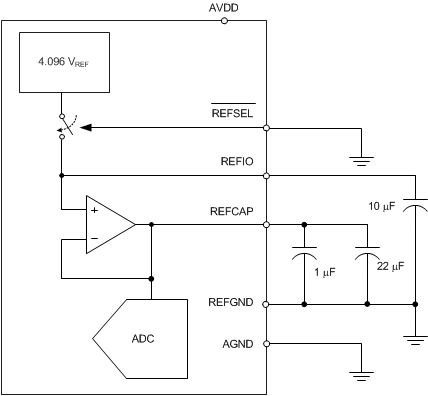 Figure 71. Device Connections for Using an Internal 4.096-V Reference
The device internal reference is trimmed to a maximum initial accuracy of ±1 mV. The histogram in Figure 72 shows the distribution of the internal voltage reference output taken from more than 3300 production devices.
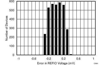 Figure 72. Internal Reference Accuracy at Room Temperature Histogram
The initial accuracy specification for the internal reference can be degraded if the die is exposed to any mechanical or thermal stress. Heating the device when being soldered to a printed circuit board (PCB) and any subsequent solder reflow is a primary cause for shifts in the VREF value. The main cause of thermal hysteresis is a change in die stress and therefore is a function of the package, die-attach material, and molding compound, as well as the layout of the device itself.
In order to illustrate this effect, 80 devices were soldered using lead-free solder paste with the manufacturer suggested reflow profile, as explained in application report SNOA550. The internal voltage reference output is measured before and after the reflow process and Figure 73 shows the typical shift in value. Although all tested units exhibit a positive shift in their output voltages, negative shifts are also possible. The histogram in Figure 73 shows the typical shift for exposure to a single reflow profile. Exposure to multiple reflows, which is common on PCBs with surface-mount components on both sides, causes additional shifts in the output voltage. If the PCB is to be exposed to multiple reflows, solder the ADS8688AT in the later pass to minimize device exposure to thermal stress.
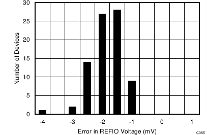 Figure 73. Solder Heat Shift Distribution Histogram
The internal reference is also temperature compensated to provide excellent temperature drift over an extended industrial temperature range of –55°C to +125°C. Figure 74 shows the variation of the internal reference voltage across temperature for different values of the AVDD supply voltage. The typical specified value of the reference voltage drift over temperature is 6 ppm/°C (Figure 75) and the maximum specified temperature drift is equal to 17 ppm/°C.
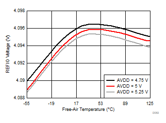
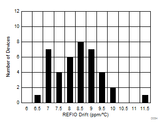
| AVDD = 5 V, number of devices = 30, ΔT = –55°C to +125°C |