SBAS813 June 2018 ADS8688AT
PRODUCTION DATA.
- 1 Features
- 2 Applications
- 3 Description
- 4 Revision History
- 5 Pin Configuration and Functions
- 6 Specifications
-
7 Detailed Description
- 7.1 Overview
- 7.2 Functional Block Diagram
- 7.3
Feature Description
- 7.3.1 Analog Inputs
- 7.3.2 Analog Input Impedance
- 7.3.3 Input Overvoltage Protection Circuit
- 7.3.4 Programmable Gain Amplifier (PGA)
- 7.3.5 Second-Order, Low-Pass Filter (LPF)
- 7.3.6 ADC Driver
- 7.3.7 Multiplexer (MUX)
- 7.3.8 Reference
- 7.3.9 Auxiliary Channel
- 7.3.10 ADC Transfer Function
- 7.3.11 Alarm Feature
- 7.4
Device Functional Modes
- 7.4.1 Device Interface
- 7.4.2
Device Modes
- 7.4.2.1 Continued Operation in the Selected Mode (NO_OP)
- 7.4.2.2 Frame Abort Condition (FRAME_ABORT)
- 7.4.2.3 STANDBY Mode (STDBY)
- 7.4.2.4 Power-Down Mode (PWR_DN)
- 7.4.2.5 Auto Channel Enable With Reset (AUTO_RST)
- 7.4.2.6 Manual Channel n Select (MAN_Ch_n)
- 7.4.2.7 Channel Sequencing Modes
- 7.4.2.8 Reset Program Registers (RST)
- 7.5
Register Maps
- 7.5.1 Command Register Description
- 7.5.2
Program Register Description
- 7.5.2.1 Program Register Read/Write Operation
- 7.5.2.2 Program Register Map
- 7.5.2.3
Program Register Descriptions
- 7.5.2.3.1 Auto-Scan Sequencing Control Registers
- 7.5.2.3.2 Device Features Selection Control Register (address = 03h)
- 7.5.2.3.3 Range Select Registers (addresses 05h-0Ch)
- 7.5.2.3.4 Alarm Flag Registers (Read-Only)
- 7.5.2.3.5
Alarm Threshold Setting Registers
- Table 22. Channel n Hysteresis Register Field Descriptions (n = 0 to 7)
- Table 23. Channel n High Threshold MSB Register Field Descriptions (n = 0 to 7)
- Table 24. Channel n High Threshold LSB Register Field Descriptions (n = 0 to 7)
- Table 25. Channel n Low Threshold MSB Register Field Descriptions (n = 0 to 7)
- Table 26. Channel n Low Threshold MSB Register Field Descriptions (n = 0 to 7)
- 7.5.2.3.6 Command Read-Back Register (address = 3Fh)
- 8 Application and Implementation
- 9 Power Supply Recommendations
- 10Layout
- 11Device and Documentation Support
- 12Mechanical, Packaging, and Orderable Information
Package Options
Mechanical Data (Package|Pins)
- DBT|38
Thermal pad, mechanical data (Package|Pins)
Orderable Information
7.4.1.3.2 Star Topology
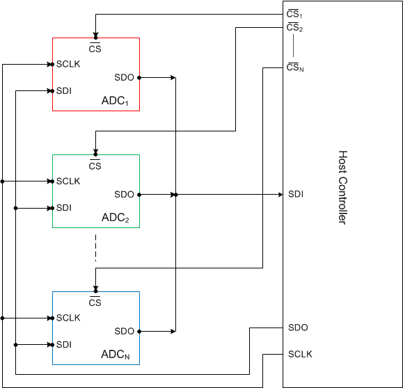
Figure 90 shows a typical connection diagram with multiple devices in the star topology. The SDI and SCLK inputs of all devices are connected together and are controlled by a single SDO and SCLK pin of the host controller, respectively. Similarly, the SDO outputs of all devices are tied together and connected to the SDI input pin of the host controller. The CS input pin of each device is individually controlled by separate CS control lines from the host controller.
 Figure 90. Star Topology Connection Schematic
The timing diagram for a typical data frame in the star topology is the same as in a stand-alone device operation, as illustrated in Figure 87. The data frame for a particular device starts with the falling edge of the CS signal and ends when the CS signal goes high. Because the host controller provides separate CS control signals for each device in this topology, devices can be selected in any order and conversions can be initiated by bringing down the CS signal for that particular device. As explained in Figure 87, when CS goes high at the end of each data frame, the SDO output of the device is placed into a Hi-Z state. Therefore, the shared SDO line in the star topology is controlled only by the device with an active data frame (CS is low). In order to avoid any conflict related to multiple devices driving the SDO line at the same time, ensure that the host controller pulls down the CS signal for only one device at any particular time.
TI recommends connecting a maximum of four devices in the star topology. Beyond that, loading may increase on the shared output lines from the host controller (SDO and SCLK). This loading can lead to digital timing errors. This limitation can be overcome by using digital buffers on the shared outputs from the host controller before being fed into additional devices.