SBAS813 June 2018 ADS8688AT
PRODUCTION DATA.
- 1 Features
- 2 Applications
- 3 Description
- 4 Revision History
- 5 Pin Configuration and Functions
- 6 Specifications
-
7 Detailed Description
- 7.1 Overview
- 7.2 Functional Block Diagram
- 7.3
Feature Description
- 7.3.1 Analog Inputs
- 7.3.2 Analog Input Impedance
- 7.3.3 Input Overvoltage Protection Circuit
- 7.3.4 Programmable Gain Amplifier (PGA)
- 7.3.5 Second-Order, Low-Pass Filter (LPF)
- 7.3.6 ADC Driver
- 7.3.7 Multiplexer (MUX)
- 7.3.8 Reference
- 7.3.9 Auxiliary Channel
- 7.3.10 ADC Transfer Function
- 7.3.11 Alarm Feature
- 7.4
Device Functional Modes
- 7.4.1 Device Interface
- 7.4.2
Device Modes
- 7.4.2.1 Continued Operation in the Selected Mode (NO_OP)
- 7.4.2.2 Frame Abort Condition (FRAME_ABORT)
- 7.4.2.3 STANDBY Mode (STDBY)
- 7.4.2.4 Power-Down Mode (PWR_DN)
- 7.4.2.5 Auto Channel Enable With Reset (AUTO_RST)
- 7.4.2.6 Manual Channel n Select (MAN_Ch_n)
- 7.4.2.7 Channel Sequencing Modes
- 7.4.2.8 Reset Program Registers (RST)
- 7.5
Register Maps
- 7.5.1 Command Register Description
- 7.5.2
Program Register Description
- 7.5.2.1 Program Register Read/Write Operation
- 7.5.2.2 Program Register Map
- 7.5.2.3
Program Register Descriptions
- 7.5.2.3.1 Auto-Scan Sequencing Control Registers
- 7.5.2.3.2 Device Features Selection Control Register (address = 03h)
- 7.5.2.3.3 Range Select Registers (addresses 05h-0Ch)
- 7.5.2.3.4 Alarm Flag Registers (Read-Only)
- 7.5.2.3.5
Alarm Threshold Setting Registers
- Table 22. Channel n Hysteresis Register Field Descriptions (n = 0 to 7)
- Table 23. Channel n High Threshold MSB Register Field Descriptions (n = 0 to 7)
- Table 24. Channel n High Threshold LSB Register Field Descriptions (n = 0 to 7)
- Table 25. Channel n Low Threshold MSB Register Field Descriptions (n = 0 to 7)
- Table 26. Channel n Low Threshold MSB Register Field Descriptions (n = 0 to 7)
- 7.5.2.3.6 Command Read-Back Register (address = 3Fh)
- 8 Application and Implementation
- 9 Power Supply Recommendations
- 10Layout
- 11Device and Documentation Support
- 12Mechanical, Packaging, and Orderable Information
Package Options
Mechanical Data (Package|Pins)
- DBT|38
Thermal pad, mechanical data (Package|Pins)
Orderable Information
7.4.2.7 Channel Sequencing Modes
The device offers two channel sequencing modes: AUTO_RST and MAN_Ch_n.
In AUTO_RST mode, the channel number automatically increments in every subsequent frame. As explained in the auto-scan sequencing control registers, the analog inputs can be selected for an automatic scan with a register setting. The device automatically scans only the selected analog inputs in ascending order. The unselected analog input channels can also be powered down for optimizing power consumption in this mode of operation. The auto-mode sequence can be reset at any time during an automatic scan (using the AUTO_RST command). When the reset command is received, the ongoing auto-mode sequence is reset and restarts from the lowest selected channel in the sequence.
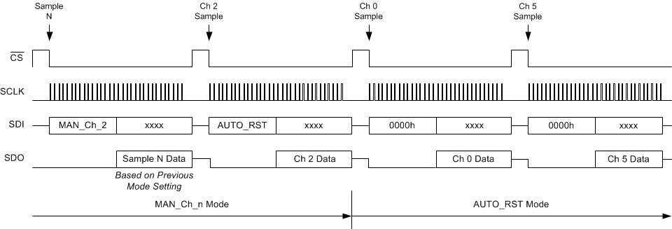
In MAN_Ch_n mode, the same input channel is selected during every data conversion frame. The input command words to select individual analog channels in MAN_Ch_n mode are listed in Table 7. If a particular input channel is selected during a data frame, then the analog inputs on the same channel are sampled during the next data frame. Figure 100 shows the SDI command sequence for transitions from AUTO_RST to MAN_Ch_n mode.
 Figure 100. Transitioning From AUTO_RST to MAN_Ch_n Mode
(Channels 0 and 5 are Selected for Auto Sequence)
Figure 101 shows the SDI command sequence for transitions from MAN_Ch_n to AUTO_RST mode. Each SDI command is executed on the next CS falling edge. A RST command can be issued at any instant during any channel sequencing mode, after which the device is placed into a default power-up state in the next data frame.
 Figure 101. Transitioning From MAN_Ch_n to AUTO_RST Mode
(Channels 0 and 5 are Selected for Auto Sequence)