SBAS813 June 2018 ADS8688AT
PRODUCTION DATA.
- 1 Features
- 2 Applications
- 3 Description
- 4 Revision History
- 5 Pin Configuration and Functions
- 6 Specifications
-
7 Detailed Description
- 7.1 Overview
- 7.2 Functional Block Diagram
- 7.3
Feature Description
- 7.3.1 Analog Inputs
- 7.3.2 Analog Input Impedance
- 7.3.3 Input Overvoltage Protection Circuit
- 7.3.4 Programmable Gain Amplifier (PGA)
- 7.3.5 Second-Order, Low-Pass Filter (LPF)
- 7.3.6 ADC Driver
- 7.3.7 Multiplexer (MUX)
- 7.3.8 Reference
- 7.3.9 Auxiliary Channel
- 7.3.10 ADC Transfer Function
- 7.3.11 Alarm Feature
- 7.4
Device Functional Modes
- 7.4.1 Device Interface
- 7.4.2
Device Modes
- 7.4.2.1 Continued Operation in the Selected Mode (NO_OP)
- 7.4.2.2 Frame Abort Condition (FRAME_ABORT)
- 7.4.2.3 STANDBY Mode (STDBY)
- 7.4.2.4 Power-Down Mode (PWR_DN)
- 7.4.2.5 Auto Channel Enable With Reset (AUTO_RST)
- 7.4.2.6 Manual Channel n Select (MAN_Ch_n)
- 7.4.2.7 Channel Sequencing Modes
- 7.4.2.8 Reset Program Registers (RST)
- 7.5
Register Maps
- 7.5.1 Command Register Description
- 7.5.2
Program Register Description
- 7.5.2.1 Program Register Read/Write Operation
- 7.5.2.2 Program Register Map
- 7.5.2.3
Program Register Descriptions
- 7.5.2.3.1 Auto-Scan Sequencing Control Registers
- 7.5.2.3.2 Device Features Selection Control Register (address = 03h)
- 7.5.2.3.3 Range Select Registers (addresses 05h-0Ch)
- 7.5.2.3.4 Alarm Flag Registers (Read-Only)
- 7.5.2.3.5
Alarm Threshold Setting Registers
- Table 22. Channel n Hysteresis Register Field Descriptions (n = 0 to 7)
- Table 23. Channel n High Threshold MSB Register Field Descriptions (n = 0 to 7)
- Table 24. Channel n High Threshold LSB Register Field Descriptions (n = 0 to 7)
- Table 25. Channel n Low Threshold MSB Register Field Descriptions (n = 0 to 7)
- Table 26. Channel n Low Threshold MSB Register Field Descriptions (n = 0 to 7)
- 7.5.2.3.6 Command Read-Back Register (address = 3Fh)
- 8 Application and Implementation
- 9 Power Supply Recommendations
- 10Layout
- 11Device and Documentation Support
- 12Mechanical, Packaging, and Orderable Information
Package Options
Mechanical Data (Package|Pins)
- DBT|38
Thermal pad, mechanical data (Package|Pins)
Orderable Information
7.3.9 Auxiliary Channel
The device includes a single-ended auxiliary input channel (AUX_IN and AUX_GND). The AUX channel provides direct interface to an internal, high-precision, 16-bit ADC through the multiplexer because this channel does not include the front-end analog signal conditioning that the other analog input channels have. The AUX channel supports a single unipolar input range of 0 V to VREF because there is no front-end PGA. The input signal on the AUX_IN pin can vary from 0 V to VREF, whereas the AUX_GND pin must be tied to AGND.
When a conversion is initiated, the voltage between these pins is sampled directly on an internal sampling capacitor (75 pF, typical). The input current required to charge the sampling capacitor is determined by several factors, including the sampling rate, input frequency, and source impedance. For slow applications that use a low-impedance source, the inputs of the AUX channel can be directly driven. When the throughput, input frequency, or the source impedance increases, a driving amplifier must be used at the input to achieve good ac performance from the AUX channel. Some key requirements of the driving amplifier are discussed in the Input Driver for the AUX Channel section.
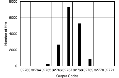
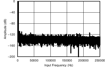
The AUX channel in the ADS8688AT offers a true 16-bit performance with no missing codes. Figure 79 and Figure 80 show some typical performance characteristics of the AUX channel.

| Mean = 32767.15, sigma = 0.83 |
(AUX Channel)

| fIN = 1 kHz, SNR = 88.2 dB, SINAD = 88.1 dB, THD = –102 dB, SFDR = 102 dB, number of points = 64k |
(AUX Channel)