SBAS813 June 2018 ADS8688AT
PRODUCTION DATA.
- 1 Features
- 2 Applications
- 3 Description
- 4 Revision History
- 5 Pin Configuration and Functions
- 6 Specifications
-
7 Detailed Description
- 7.1 Overview
- 7.2 Functional Block Diagram
- 7.3
Feature Description
- 7.3.1 Analog Inputs
- 7.3.2 Analog Input Impedance
- 7.3.3 Input Overvoltage Protection Circuit
- 7.3.4 Programmable Gain Amplifier (PGA)
- 7.3.5 Second-Order, Low-Pass Filter (LPF)
- 7.3.6 ADC Driver
- 7.3.7 Multiplexer (MUX)
- 7.3.8 Reference
- 7.3.9 Auxiliary Channel
- 7.3.10 ADC Transfer Function
- 7.3.11 Alarm Feature
- 7.4
Device Functional Modes
- 7.4.1 Device Interface
- 7.4.2
Device Modes
- 7.4.2.1 Continued Operation in the Selected Mode (NO_OP)
- 7.4.2.2 Frame Abort Condition (FRAME_ABORT)
- 7.4.2.3 STANDBY Mode (STDBY)
- 7.4.2.4 Power-Down Mode (PWR_DN)
- 7.4.2.5 Auto Channel Enable With Reset (AUTO_RST)
- 7.4.2.6 Manual Channel n Select (MAN_Ch_n)
- 7.4.2.7 Channel Sequencing Modes
- 7.4.2.8 Reset Program Registers (RST)
- 7.5
Register Maps
- 7.5.1 Command Register Description
- 7.5.2
Program Register Description
- 7.5.2.1 Program Register Read/Write Operation
- 7.5.2.2 Program Register Map
- 7.5.2.3
Program Register Descriptions
- 7.5.2.3.1 Auto-Scan Sequencing Control Registers
- 7.5.2.3.2 Device Features Selection Control Register (address = 03h)
- 7.5.2.3.3 Range Select Registers (addresses 05h-0Ch)
- 7.5.2.3.4 Alarm Flag Registers (Read-Only)
- 7.5.2.3.5
Alarm Threshold Setting Registers
- Table 22. Channel n Hysteresis Register Field Descriptions (n = 0 to 7)
- Table 23. Channel n High Threshold MSB Register Field Descriptions (n = 0 to 7)
- Table 24. Channel n High Threshold LSB Register Field Descriptions (n = 0 to 7)
- Table 25. Channel n Low Threshold MSB Register Field Descriptions (n = 0 to 7)
- Table 26. Channel n Low Threshold MSB Register Field Descriptions (n = 0 to 7)
- 7.5.2.3.6 Command Read-Back Register (address = 3Fh)
- 8 Application and Implementation
- 9 Power Supply Recommendations
- 10Layout
- 11Device and Documentation Support
- 12Mechanical, Packaging, and Orderable Information
Package Options
Mechanical Data (Package|Pins)
- DBT|38
Thermal pad, mechanical data (Package|Pins)
Orderable Information
7.3.8.2 External Reference
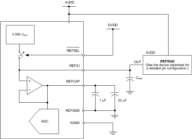
For applications that require a better reference voltage or a common reference voltage for multiple devices, the ADS8688AT offers a provision to use an external reference along with an internal buffer to drive the ADC reference pin. In order to select the external reference mode, either tie the REFSEL pin high or connect this pin to the DVDD supply. In this mode, an external 4.096-V reference must be applied at REFIO (pin 5), which becomes an input pin. Any low-power, low-drift, or small-size external reference can be used in this mode because the internal buffer is optimally designed to handle the dynamic loading on the REFCAP pin, which is internally connected to the ADC reference input. The output of the external reference must be appropriately filtered to minimize the resulting effect of the reference noise on system performance. Figure 76 shows a typical connection diagram for this mode.
 Figure 76. Device Connections for Using an External 4.096-V Reference
The output of the internal reference buffer appears at the REFCAP pin. A minimum capacitance of 10 µF must be placed between REFCAP (pin 7) and REFGND (pin 6). Place another capacitor of 1 µF as close to the REFCAP pin as possible for decoupling high-frequency signals. Do not use the internal buffer to drive external ac or dc loads because of the limited current output capability of this buffer.
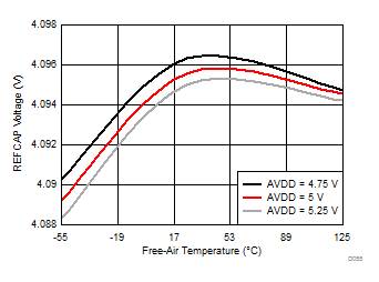
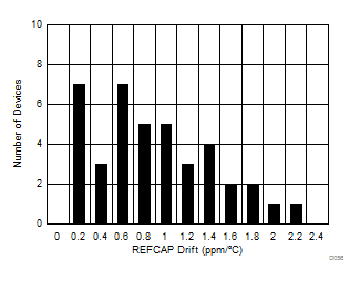
The performance of the internal buffer output is very stable across the entire operating temperature range of –55°C to +125°C. Figure 77 shows the variation in the REFCAP output across temperature for different values of the AVDD supply voltage. The typical specified value of the reference buffer drift over temperature is 0.6 ppm/°C (Figure 78) and the maximum specified temperature drift is equal to 4.5 ppm/°C.


| AVDD = 5 V, number of devices = 30, ΔT = –55°C to 125°C |