SBAS813 June 2018 ADS8688AT
PRODUCTION DATA.
- 1 Features
- 2 Applications
- 3 Description
- 4 Revision History
- 5 Pin Configuration and Functions
- 6 Specifications
-
7 Detailed Description
- 7.1 Overview
- 7.2 Functional Block Diagram
- 7.3
Feature Description
- 7.3.1 Analog Inputs
- 7.3.2 Analog Input Impedance
- 7.3.3 Input Overvoltage Protection Circuit
- 7.3.4 Programmable Gain Amplifier (PGA)
- 7.3.5 Second-Order, Low-Pass Filter (LPF)
- 7.3.6 ADC Driver
- 7.3.7 Multiplexer (MUX)
- 7.3.8 Reference
- 7.3.9 Auxiliary Channel
- 7.3.10 ADC Transfer Function
- 7.3.11 Alarm Feature
- 7.4
Device Functional Modes
- 7.4.1 Device Interface
- 7.4.2
Device Modes
- 7.4.2.1 Continued Operation in the Selected Mode (NO_OP)
- 7.4.2.2 Frame Abort Condition (FRAME_ABORT)
- 7.4.2.3 STANDBY Mode (STDBY)
- 7.4.2.4 Power-Down Mode (PWR_DN)
- 7.4.2.5 Auto Channel Enable With Reset (AUTO_RST)
- 7.4.2.6 Manual Channel n Select (MAN_Ch_n)
- 7.4.2.7 Channel Sequencing Modes
- 7.4.2.8 Reset Program Registers (RST)
- 7.5
Register Maps
- 7.5.1 Command Register Description
- 7.5.2
Program Register Description
- 7.5.2.1 Program Register Read/Write Operation
- 7.5.2.2 Program Register Map
- 7.5.2.3
Program Register Descriptions
- 7.5.2.3.1 Auto-Scan Sequencing Control Registers
- 7.5.2.3.2 Device Features Selection Control Register (address = 03h)
- 7.5.2.3.3 Range Select Registers (addresses 05h-0Ch)
- 7.5.2.3.4 Alarm Flag Registers (Read-Only)
- 7.5.2.3.5
Alarm Threshold Setting Registers
- Table 22. Channel n Hysteresis Register Field Descriptions (n = 0 to 7)
- Table 23. Channel n High Threshold MSB Register Field Descriptions (n = 0 to 7)
- Table 24. Channel n High Threshold LSB Register Field Descriptions (n = 0 to 7)
- Table 25. Channel n Low Threshold MSB Register Field Descriptions (n = 0 to 7)
- Table 26. Channel n Low Threshold MSB Register Field Descriptions (n = 0 to 7)
- 7.5.2.3.6 Command Read-Back Register (address = 3Fh)
- 8 Application and Implementation
- 9 Power Supply Recommendations
- 10Layout
- 11Device and Documentation Support
- 12Mechanical, Packaging, and Orderable Information
Package Options
Mechanical Data (Package|Pins)
- DBT|38
Thermal pad, mechanical data (Package|Pins)
Orderable Information
7.4.1.3.1 Daisy-Chain Topology
Figure 88 shows a typical connection diagram with multiple devices in daisy-chain mode. The CS, SCLK, and SDI inputs of all devices are connected together and controlled by a single CS, SCLK, and SDO pin of the host controller, respectively. The DAISY1 input pin of the first ADC in the chain is connected to DGND, the SDO1 output pin is connected to the DAISY2 input of ADC2, and so forth. The SDON pin of the Nth ADC in the chain is connected to the SDI pin of the host controller. The devices do not require any special hardware or software configuration to enter daisy-chain mode.
 Figure 88. Daisy-Chain Connection Schematic
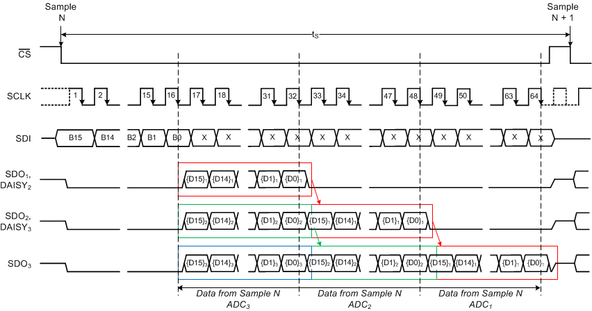
Figure 89 shows a typical timing diagram for three devices connected in daisy-chain mode.
 Figure 89. Three Devices Connected in Daisy-Chain Mode Timing Diagram
At the falling edge of the CS signal, all devices sample the input signal at their respective selected channels and enter into conversion phase. For the first 16 SCLK cycles, the internal register settings for the next conversion can be entered using the SDI line that is common to all devices in the chain. During this time period, the SDO outputs for all devices remain low. At the end of conversion, every ADC in the chain loads its own conversion result into an internal 16-bit shift register. At the 16th SCLK falling edge, every ADC in the chain outputs the MSB bit on its own SDO output pin. On every subsequent SCLK falling edge, the internal shift register of each ADC latches the data available on its DAISY pin and shifts out the next bit of data on its SDO pin. Therefore, the digital host receives the data of ADCN, followed by the data of ADCN–1, and so forth (in MSB-first fashion). In total, a minimum of 16 × N SCLK falling edges are required to capture the outputs of all N devices in the chain. This example uses three devices in a daisy-chain connection, so 3 × 16 = 48 SCLK cycles are required to capture the outputs of all devices in the chain along with the 16 SCLK cycles to input the register settings for the next conversion, resulting in a total of 64 SCLK cycles for the entire data frame. The overall throughput of the system is proportionally reduced with the number of devices connected in a daisy-chain configuration.
The following points must be noted about the daisy-chain configuration illustrated in Figure 88:
- The SDI pins for all devices are connected together so each device operates with the same internal configuration. This limitation can be overcome by spending additional host controller resources to control the CS or SDI input of devices with unique configurations.
- If the number of devices connected in daisy-chain is more than four, loading increases on the shared output lines from the host controller (CS, SDO, and SCLK). This increased loading can lead to digital timing errors. This limitation can be overcome by using digital buffers on the shared outputs from the host controller before feeding the shared digital lines into additional devices.