SBAS813 June 2018 ADS8688AT
PRODUCTION DATA.
- 1 Features
- 2 Applications
- 3 Description
- 4 Revision History
- 5 Pin Configuration and Functions
- 6 Specifications
-
7 Detailed Description
- 7.1 Overview
- 7.2 Functional Block Diagram
- 7.3
Feature Description
- 7.3.1 Analog Inputs
- 7.3.2 Analog Input Impedance
- 7.3.3 Input Overvoltage Protection Circuit
- 7.3.4 Programmable Gain Amplifier (PGA)
- 7.3.5 Second-Order, Low-Pass Filter (LPF)
- 7.3.6 ADC Driver
- 7.3.7 Multiplexer (MUX)
- 7.3.8 Reference
- 7.3.9 Auxiliary Channel
- 7.3.10 ADC Transfer Function
- 7.3.11 Alarm Feature
- 7.4
Device Functional Modes
- 7.4.1 Device Interface
- 7.4.2
Device Modes
- 7.4.2.1 Continued Operation in the Selected Mode (NO_OP)
- 7.4.2.2 Frame Abort Condition (FRAME_ABORT)
- 7.4.2.3 STANDBY Mode (STDBY)
- 7.4.2.4 Power-Down Mode (PWR_DN)
- 7.4.2.5 Auto Channel Enable With Reset (AUTO_RST)
- 7.4.2.6 Manual Channel n Select (MAN_Ch_n)
- 7.4.2.7 Channel Sequencing Modes
- 7.4.2.8 Reset Program Registers (RST)
- 7.5
Register Maps
- 7.5.1 Command Register Description
- 7.5.2
Program Register Description
- 7.5.2.1 Program Register Read/Write Operation
- 7.5.2.2 Program Register Map
- 7.5.2.3
Program Register Descriptions
- 7.5.2.3.1 Auto-Scan Sequencing Control Registers
- 7.5.2.3.2 Device Features Selection Control Register (address = 03h)
- 7.5.2.3.3 Range Select Registers (addresses 05h-0Ch)
- 7.5.2.3.4 Alarm Flag Registers (Read-Only)
- 7.5.2.3.5
Alarm Threshold Setting Registers
- Table 22. Channel n Hysteresis Register Field Descriptions (n = 0 to 7)
- Table 23. Channel n High Threshold MSB Register Field Descriptions (n = 0 to 7)
- Table 24. Channel n High Threshold LSB Register Field Descriptions (n = 0 to 7)
- Table 25. Channel n Low Threshold MSB Register Field Descriptions (n = 0 to 7)
- Table 26. Channel n Low Threshold MSB Register Field Descriptions (n = 0 to 7)
- 7.5.2.3.6 Command Read-Back Register (address = 3Fh)
- 8 Application and Implementation
- 9 Power Supply Recommendations
- 10Layout
- 11Device and Documentation Support
- 12Mechanical, Packaging, and Orderable Information
Package Options
Mechanical Data (Package|Pins)
- DBT|38
Thermal pad, mechanical data (Package|Pins)
Orderable Information
8.2.2.3 Application Curve
Table 29 summarizes the performance for this design.
Table 29. Measurement Results Summary for PLC Analog Input Module Design
| SERIAL NUMBER | PARAMETER | INPUT RANGE | ADS8688AT SPECIFICATION | MEASURED RESULT |
|---|---|---|---|---|
| 1 | SNR (dB) | ±10 V | 90 dB (min) | 90.85 dB |
| 0 V 10 V | 88.5 dB (min) | 89.52 dB | ||
| 0 V to 5 V | 87.5 dB (min) | 88.48 dB | ||
| 2 | ENOB (Bits) | ±10 V | 14.66 | 14.80 |
| 0 V 10 V | 14.41 | 14.58 | ||
| 0 V to 5 V | 14.24 | 14.41 | ||
| 3 | Maximum INL (LSB) | ±10 V | 2 | 1.77 |
| 0 V 10 V | 2 | 1.64 | ||
| 0 V to 5 V | 2 | 1.35 | ||
| 4 | Minimum INL (LSB) | ±10 V | –2 | –1.47 |
| 0 V 10 V | –2 | –1.36 | ||
| 0 V to 5 V | –2 | –1.37 |
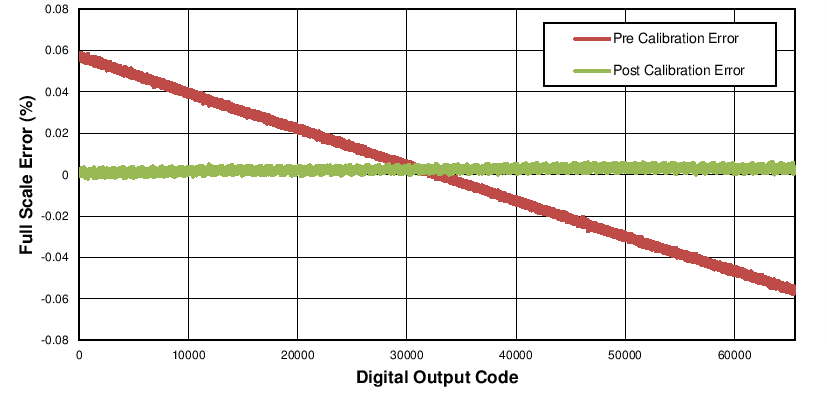
Figure 123 shows the accuracy performance for this design for the ±10.24-V input range.
 Figure 123. System Accuracy Performance in ±2.5 × VREF Input Range

|
For a step-by-step design procedure, circuit schematics, bill of materials, PCB files, simulation results, and test results, see 16-Bit, 8-Channel, Integrated Analog Input Module for Programmable Logic Controllers (PLCs). |