SBAS813 June 2018 ADS8688AT
PRODUCTION DATA.
- 1 Features
- 2 Applications
- 3 Description
- 4 Revision History
- 5 Pin Configuration and Functions
- 6 Specifications
-
7 Detailed Description
- 7.1 Overview
- 7.2 Functional Block Diagram
- 7.3
Feature Description
- 7.3.1 Analog Inputs
- 7.3.2 Analog Input Impedance
- 7.3.3 Input Overvoltage Protection Circuit
- 7.3.4 Programmable Gain Amplifier (PGA)
- 7.3.5 Second-Order, Low-Pass Filter (LPF)
- 7.3.6 ADC Driver
- 7.3.7 Multiplexer (MUX)
- 7.3.8 Reference
- 7.3.9 Auxiliary Channel
- 7.3.10 ADC Transfer Function
- 7.3.11 Alarm Feature
- 7.4
Device Functional Modes
- 7.4.1 Device Interface
- 7.4.2
Device Modes
- 7.4.2.1 Continued Operation in the Selected Mode (NO_OP)
- 7.4.2.2 Frame Abort Condition (FRAME_ABORT)
- 7.4.2.3 STANDBY Mode (STDBY)
- 7.4.2.4 Power-Down Mode (PWR_DN)
- 7.4.2.5 Auto Channel Enable With Reset (AUTO_RST)
- 7.4.2.6 Manual Channel n Select (MAN_Ch_n)
- 7.4.2.7 Channel Sequencing Modes
- 7.4.2.8 Reset Program Registers (RST)
- 7.5
Register Maps
- 7.5.1 Command Register Description
- 7.5.2
Program Register Description
- 7.5.2.1 Program Register Read/Write Operation
- 7.5.2.2 Program Register Map
- 7.5.2.3
Program Register Descriptions
- 7.5.2.3.1 Auto-Scan Sequencing Control Registers
- 7.5.2.3.2 Device Features Selection Control Register (address = 03h)
- 7.5.2.3.3 Range Select Registers (addresses 05h-0Ch)
- 7.5.2.3.4 Alarm Flag Registers (Read-Only)
- 7.5.2.3.5
Alarm Threshold Setting Registers
- Table 22. Channel n Hysteresis Register Field Descriptions (n = 0 to 7)
- Table 23. Channel n High Threshold MSB Register Field Descriptions (n = 0 to 7)
- Table 24. Channel n High Threshold LSB Register Field Descriptions (n = 0 to 7)
- Table 25. Channel n Low Threshold MSB Register Field Descriptions (n = 0 to 7)
- Table 26. Channel n Low Threshold MSB Register Field Descriptions (n = 0 to 7)
- 7.5.2.3.6 Command Read-Back Register (address = 3Fh)
- 8 Application and Implementation
- 9 Power Supply Recommendations
- 10Layout
- 11Device and Documentation Support
- 12Mechanical, Packaging, and Orderable Information
Package Options
Mechanical Data (Package|Pins)
- DBT|38
Thermal pad, mechanical data (Package|Pins)
Orderable Information
7.4.2.3 STANDBY Mode (STDBY)
The device supports a low-power standby mode (STDBY) in which only part of the circuit is powered down. The internal reference and buffer is not powered down, and therefore, the device can be quickly powered up in 20 µs on exiting the STDBY mode. When the device comes out of STDBY mode, the program registers are not reset to the default values.
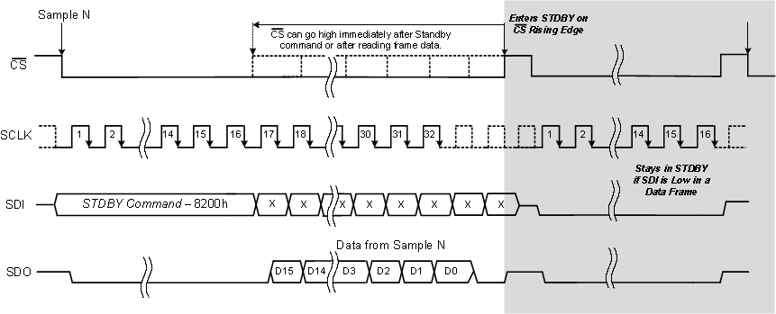
To enter STDBY mode, execute a valid write operation as shown in Figure 92 to the command register with a STDBY command of 8200h. The command is executed and the device enters STDBY mode on the next CS rising edge following this write operation. The device remains in STDBY mode if no valid conversion command (AUTO_RST or MAN_Ch_n) is executed and SDI remains low (see the Continued Operation in the Selected Mode (NO_OP) section) during the subsequent data frames. When the device operates in STDBY mode, the program register settings can be updated (as explained in the Program Register Read/Write Operation section) using 16 SCLK cycles. However, if 32 complete SCLK cycles are provided, then the device returns invalid data on the SDO line because there is no ongoing conversion in STDBY mode. The program register read operation can take place normally during this mode.
 Figure 92. Enter and Remain in STDBY Mode Timing Diagram
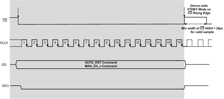
In order to exit STDBY mode, as shown in Figure 93, a valid 16-bit write command must be executed to enter auto (AUTO_RST) or manual (MAN_CH_n) scan mode. The device starts exiting STDBY mode on the next CS rising edge. At the next CS falling edge, the device samples the analog input at the channel selected by the MAN_CH_n command or the first channel of the AUTO_RST mode sequence. To ensure that the input signal is sampled correctly, keep the minimum width of the CS signal at 20 µs after exiting STDBY mode so the device internal circuitry can be fully powered up and biased properly before taking the sample. The data output for the selected channel can be read during the same data frame, as explained in Figure 87.
 Figure 93. Exit STDBY Mode Timing Diagram