SBAS813 June 2018 ADS8688AT
PRODUCTION DATA.
- 1 Features
- 2 Applications
- 3 Description
- 4 Revision History
- 5 Pin Configuration and Functions
- 6 Specifications
-
7 Detailed Description
- 7.1 Overview
- 7.2 Functional Block Diagram
- 7.3
Feature Description
- 7.3.1 Analog Inputs
- 7.3.2 Analog Input Impedance
- 7.3.3 Input Overvoltage Protection Circuit
- 7.3.4 Programmable Gain Amplifier (PGA)
- 7.3.5 Second-Order, Low-Pass Filter (LPF)
- 7.3.6 ADC Driver
- 7.3.7 Multiplexer (MUX)
- 7.3.8 Reference
- 7.3.9 Auxiliary Channel
- 7.3.10 ADC Transfer Function
- 7.3.11 Alarm Feature
- 7.4
Device Functional Modes
- 7.4.1 Device Interface
- 7.4.2
Device Modes
- 7.4.2.1 Continued Operation in the Selected Mode (NO_OP)
- 7.4.2.2 Frame Abort Condition (FRAME_ABORT)
- 7.4.2.3 STANDBY Mode (STDBY)
- 7.4.2.4 Power-Down Mode (PWR_DN)
- 7.4.2.5 Auto Channel Enable With Reset (AUTO_RST)
- 7.4.2.6 Manual Channel n Select (MAN_Ch_n)
- 7.4.2.7 Channel Sequencing Modes
- 7.4.2.8 Reset Program Registers (RST)
- 7.5
Register Maps
- 7.5.1 Command Register Description
- 7.5.2
Program Register Description
- 7.5.2.1 Program Register Read/Write Operation
- 7.5.2.2 Program Register Map
- 7.5.2.3
Program Register Descriptions
- 7.5.2.3.1 Auto-Scan Sequencing Control Registers
- 7.5.2.3.2 Device Features Selection Control Register (address = 03h)
- 7.5.2.3.3 Range Select Registers (addresses 05h-0Ch)
- 7.5.2.3.4 Alarm Flag Registers (Read-Only)
- 7.5.2.3.5
Alarm Threshold Setting Registers
- Table 22. Channel n Hysteresis Register Field Descriptions (n = 0 to 7)
- Table 23. Channel n High Threshold MSB Register Field Descriptions (n = 0 to 7)
- Table 24. Channel n High Threshold LSB Register Field Descriptions (n = 0 to 7)
- Table 25. Channel n Low Threshold MSB Register Field Descriptions (n = 0 to 7)
- Table 26. Channel n Low Threshold MSB Register Field Descriptions (n = 0 to 7)
- 7.5.2.3.6 Command Read-Back Register (address = 3Fh)
- 8 Application and Implementation
- 9 Power Supply Recommendations
- 10Layout
- 11Device and Documentation Support
- 12Mechanical, Packaging, and Orderable Information
Package Options
Mechanical Data (Package|Pins)
- DBT|38
Thermal pad, mechanical data (Package|Pins)
Orderable Information
7.4.1.2 Data Acquisition Example
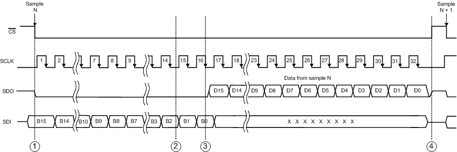
This section provides an example of how a host processor can use the device interface to configure the device internal registers as well as convert and acquire data for sampling a particular input channel. The timing diagram shown in Figure 87 provides further details.
 Figure 87. Device Operation Using the Serial Interface Timing Diagram
There are four events shown in Figure 87, which are described below:
- Event 1: The host initiates a data conversion frame through a falling edge of the CS signal. The analog input signal at the instant of the CS falling edge is sampled by the ADC and conversion is performed using an internal oscillator clock. The analog input channel converted during this frame is selected in the previous data frame. The internal register settings of the device for the next conversion can be input during this data frame using the SDI and SCLK inputs. Initiate SCLK at this instant and latch data on the SDI line into the device on every SCLK falling edge for the next 16 SCLK cycles. At this instant, SDO goes low because the device does not output internal conversion data on the SDO line during the first 16 SCLK cycles.
- Event 2: During the first 16 SCLK cycles, the device completes the internal conversion process and data are now ready within the converter. However, the device does not output data bits on SDO until the 16th falling edge appears on the SCLK input. Because the ADC conversion time is fixed (the maximum value is given in the Electrical Characteristics table), the 16th SCLK falling edge must appear after the internal conversion is over, otherwise data output from the device is incorrect. Therefore, the SCLK frequency cannot exceed a maximum value, as provided in the Timing Requirements: Serial Interface table.
- Event 3: At the 16th falling edge of the SCLK signal, the device reads the LSB of the input word on the SDI line. The device does not read anything from the SDI line for the remaining data frame. On the same edge, the MSB of the conversion data is output on the SDO line and can be read by the host processor on the subsequent falling edge of the SCLK signal. For 16 bits of output data, the LSB can be read on the 32nd SCLK falling edge. The SDO outputs 0 on subsequent SCLK falling edges until the next conversion is initiated.
- Event 4: When the internal data from the device is received, the host terminates the data frame by deactivating the CS signal to high. The SDO output goes into a Hi-Z state until the next data frame is initiated, as explained in Event 1.